
Semiconductor integrated circuit and method of designing thereof based on TPI

a technology of integrated circuit and semiconductor, applied in the direction of software simulation/interpretation/emulation, instruments, program control, etc., can solve the problems of increasing circuit malfunction, and the increase of the malfunction caused by the small delay defect, so as to reduce avoid unnecessary increase in the number of test points, and reduce the overlook of the small delay defect

Inactive Publication Date: 2011-11-08
RENESAS ELECTRONICS CORP
View PDF12 Cites 5 Cited by
  • Summary
  • Abstract
  • Description
  • Claims
  • Application Information

AI Technical Summary

Benefits of technology

This approach reduces the occurrence of overlooked small delay defects, enhances product reliability, and minimizes the number of test points needed, thereby reducing overhead and costs associated with chip area and testing time.

Problems solved by technology

With speeding up and increasing miniaturization of semiconductor manufacturing processes, even a small deviation from a design value in the critical path can cause the circuit to malfunction.
That is to say, malfunction caused by the small delay defect has been increasing with speeding up and increasing miniaturization of the circuit.
Such a defect that does not affect the system operation is called a timing redundant defect.
Therefore, the delay defect is not detected but overlooked in the delay testing.
However, which path is used in the delay testing depends on the ATPG, and there is generally a tendency that a relatively short path is used.
Therefore, the small delay defect is likely to be overlooked in the delay testing.
In this case, however, the ATPG needs to generate test patterns with searching for the longest path in order to achieve the defect detection using the longest path, and thus the time for generating the test patterns becomes much longer.
Moreover, constraint on signal values for testing the longest path is increased as compared with the common ATPG, which leads to increase in the number of test patterns.
These cause increase in the time and cost of the delay testing.
Therefore, the small delay defect is likely to be overlooked in the delay testing.
As described above, the small delay defect is likely to be overlooked in the delay testing, in the case of the typical TPI technique in which the path delay is not considered.
The existing design technique does not support the detection of the small delay defect.
If the small delay defect is overlooked during the test, a malfunction occurrence rate in the market is increased, which leads to deterioration of the product reliability.

Method used


Image

  • Semiconductor integrated circuit and method of designing thereof based on TPI
  • Semiconductor integrated circuit and method of designing thereof based on TPI
  • Semiconductor integrated circuit and method of designing thereof based on TPI

Examples


first example

2-1. FIRST EXAMPLE

[0045]FIG. 5 shows a first example of the design circuit according to the present embodiment. The design circuit shown in FIG. 5 includes flip-flops (scan flip-flops) FF1 to FF4, as in the case shown in FIG. 1. As shown in FIG. 5, a test point TP (observation flip-flop) is inserted at a target node TN within the design circuit. A path from the flip-flop FF1 to the test point TP is the test point path PT. The longest path, whose delay time is the maximum among paths other than the test point path PT passing through the target node TN, is the path P2 (delay time: 8 ns) from the flip-flop FF1 to the flip-flop FF4.

[0046]In Step S200, a TP delay is designated with respect to the test point path PT. In the first example, the delay time (8 ns) of the longest path P2 is designated as the TP delay. In other words, the TP delay is set to be equal to the delay time of the longest path P2 that would be a preferable path used in the delay testing if the test point TP is not ins...

second example

2-2. SECOND EXAMPLE

[0048]FIG. 6 shows a second example of the design circuit according to the present embodiment. The description overlapping with the first example will be omitted as appropriate. In the second example, a test clock cycle (test timing) at the time of the delay testing is designated as the TP delay. In the present example, the test clock cycle is 9 ns and thus the TP delay is set to 9 ns. The TP delay is the maximum among delay times of paths passing through the target node TN. In order that the designated TP delay is achieved, some inverters as delay elements are inserted as shown in FIG. 6. As a result, the test point path PT with delay time of 9 ns is obtained.

[0049]The test point path PT is used in the delay testing. Therefore, even if a small delay defect occurs at the target node TN, the small delay defect is not overlooked but detected precisely. That is, the same effect as in the first example can be obtained. Moreover, the detection accuracy of the small del...

third example

2-3. THIRD EXAMPLE

[0051]In the foregoing examples, the cases of the observation test point have been explained. The same applies to a case of a control test point. FIG. 7 shows an example of a case where a control test point is inserted. A design circuit shown in FIG. 7 includes flip-flops (scan flip-flops) FF5 to FF8. Also, a test point TP (control flip-flop) is inserted at a target node TN. A path from the test point TP to the flip-flop FF8 is the test point path PT. A certain TP delay is designated with respect to the test point path PT. For example, the TP delay is set to be equal to a delay time of the longest path P5 passing through the target node TN. Alternatively, the TP delay may be set to be equal to the test clock cycle at the time of the delay testing.

[0052]3. Method of Determining Test Point Insertion Position

[0053]As described above, the test point TP according to the present embodiment can support detection of the small delay defect. Next, a method of determining whe...


PUM


Abstract

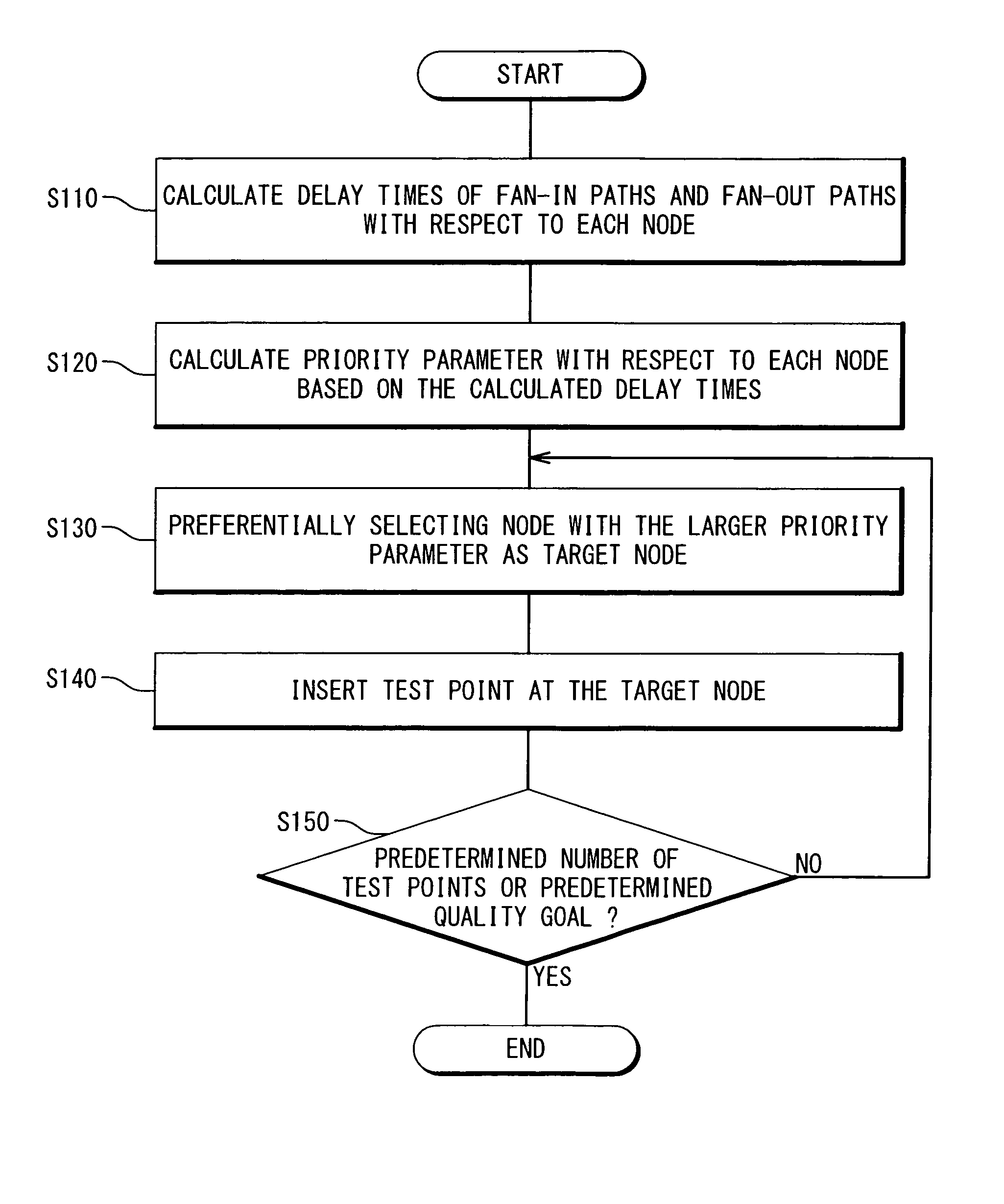
A method of designing a semiconductor integrated circuit based on the TPI technique, comprising: (A) selecting a target node from a plurality of nodes included in a design circuit; (B) inserting a test point at the target node; (C) designating a delay time with respect to a test point path that is a path connected to the test point; and (D) laying out the design circuit such that a delay time of the test point path becomes the designated delay time. The (A) selecting includes: (A1) calculating delay times of fan-in paths and fan-out paths with respect to each of the plurality of nodes; and (A2) selecting the target node from the plurality of nodes based on the calculated delay times.

Description

BACKGROUND OF THE INVENTION[0001]1. Field of the Invention[0002]The present invention relates to a technique of designing a semiconductor integrated circuit. In particular, the present invention relates to a technique of designing a semiconductor integrated circuit by using a TPI (Test Point Insertion) method.[0003]This application is based upon and claims the benefit of priority from Japanese patent application No. 2007-135358, filed on May 22, 2007, the disclosure of which is incorporated herein in its entirely by reference.[0004]2. Description of Related Art[0005]After a semiconductor integrated circuit is manufactured, it is necessary to conduct a test for checking whether or not defects such as a delay fault (delay defect) and a stuck-at fault occur in the product. It is therefore preferable to build a test circuit that can enhance testability of the testing into the semiconductor integrated circuit in advance during a circuit design stage. Such a design technique is called “DF...

Claims


Application Information

Patent Timeline
Patent Type & Authority Patents(United States)
IPC IPC(8): G06F9/455G06F17/50
CPCG01R31/318583
Inventor MAEDA, TOSHIYUKIASAKA, TOSHIHARU
Owner RENESAS ELECTRONICS CORP
Learn More