
Multilayer chip capacitor and circuit board device including the same

a multi-layer chip and capacitor technology, applied in the direction of fixed capacitor details, sustainable manufacturing/processing, final product manufacturing, etc., can solve the problem of sudden change of voltage, deterioration of stability, and difficulty in suppressing noise of direct-current supply voltage (dc) voltag

Active Publication Date: 2011-11-01
SAMSUNG ELECTRO MECHANICS CO LTD
View PDF37 Cites 8 Cited by
  • Summary
  • Abstract
  • Description
  • Claims
  • Application Information

AI Technical Summary

Benefits of technology

[0024]Vias connected to the first and second pads may be formed in the circuit board, as a portion of the external circuit. To reduce a current loop size flowing through the first capacitor part via the first and second pads, the via connected to the first pad may be disposed adjacent to the second pad, and the via connected to the second pad may be disposed adjacent to the first pad. Two or more of the vias may be connected to each of the first and second pads, respectively.
[0030]According to an exemplary embodiment of the present invention, there is provided a multilayer chip capacitor capable of embodying a low ESL and maintaining a suitable ESR. When applying the multilayer chip capacitor to a decoupling application, it is possible to maintain an impedance of a power distribution network to be low and uniform within a wide frequency band, thereby providing a decoupling capacitor with a high and controllable ESR and a low ESL.

Problems solved by technology

Accordingly, it becomes more difficult to suppress noise of a supply direct-current (DC) voltage according to a sudden change of a consumed current of an MPU.
An excessively small ESR deteriorates the stability of a power supply circuit, thereby suddenly changing a voltage due to power network resonance.
However, due to the excessively small ESR, it is difficult to maintain the magnitude of an impedance of a power distribution network to be low and uniform.
However, when using high-resistance outer electrodes, it is difficult to prevent localized heat spots caused by a current concentration phenomenon due to pinholes in outer electrodes and to accurately control ESR.
Also, when using high-resistance materials for inner electrodes, disadvantageously, high-resistant internal electrode materials should be changed with the improvement or change of ceramic materials since the high-resistant internal electrode materials should be matched with the ceramic materials, which leads to the increased cost of the products.
However, as disclosed, it is impossible to maintain an impedance to be uniform around each resonating frequency, thereby having a harmful effect on stability of a power supply circuit.

Method used


Image

  • Multilayer chip capacitor and circuit board device including the same
  • Multilayer chip capacitor and circuit board device including the same
  • Multilayer chip capacitor and circuit board device including the same

Examples


##ventive example 1

Inventive Example 1

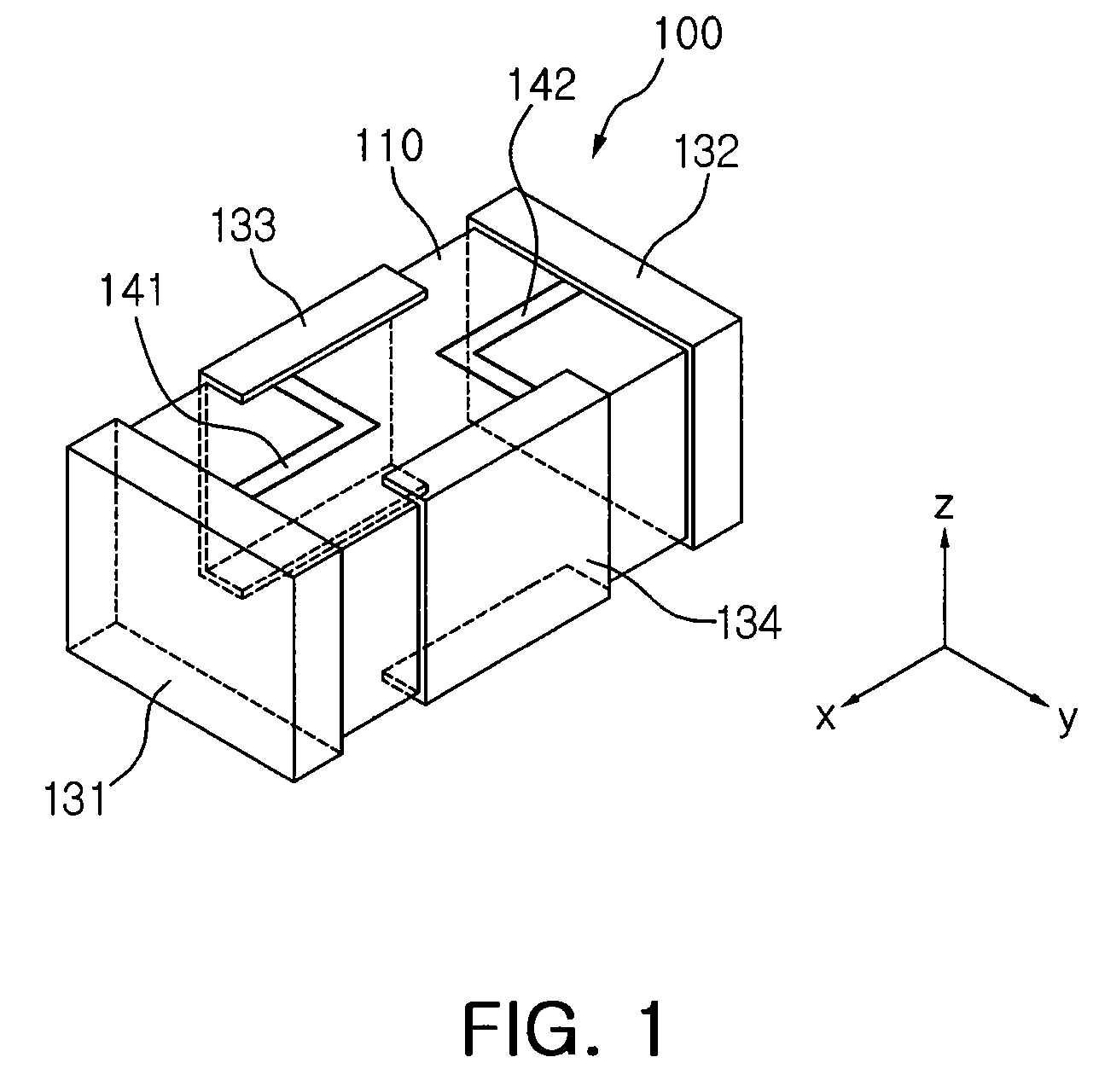
[0118]FIG. 32 is a graph illustrating frequency-to-impedance characteristics of multilayer chip capacitors according to inventive example 1 and a comparative example. An impedance curve a of the multilayer chip capacitor according to the inventive example 1 shows a result of experiments of measuring a frequency and an impedance of the multilayer chip capacitor 100 and the circuit board device of FIGS. 1 to 5.

[0119]Particularly, the inventive example 1 corresponds to a multilayer chip capacitor of a four-terminal capacitor with a capacitance of 10 μF and a size of 1608 (1.6 mm×0.8 mm). A capacitance of a first capacitor part is 1.73 μF, and a capacitance of a second capacitor part is 8.27 μF. Also, an ESL and an ESR of the first capacitor part are 350 pH and 38 mΩ, respectively. Actual ESL and ESR of conduction conductor lines and the whole second capacitor part (L2′ and R2′ of FIG. 6) are 2200 pH and 40 mΩ, respectively. As described above, regardless of a great c...

##ventive example 2

Inventive Example 2

[0123]FIG. 33 is a graph illustrating frequency-to-impedance characteristics of multilayer chip capacitors according to inventive example 2 and the comparative example. An impedance curve c of the multilayer chip capacitor according to the inventive example 2 shows a result of experiments of measuring a frequency and an impedance of the multilayer chip capacitor 200 and the circuit board device of FIGS. 17 to 21.

[0124]Particularly, the inventive example 2 corresponds to a multilayer chip capacitor of a four-terminal capacitor with a capacitance of 10 μF and a size of 1608 (1.6 mm×0.8 mm). A capacitance of a first capacitor part is 0.52 μF, and a capacitance of a second capacitor part is 9.48 μF. Also, an ESL and an ESR of the first capacitor part are 300 pH and 60 mΩ, respectively. Actual ESL and ESR of conduction conductor lines and the whole second capacitor part (L2′ and R2′ of FIG. 6) are 700 pH and 35 mΩ, respectively.

[0125]Averaged ESLs and minimum impedance...


PUM


Abstract

A multilayer chip capacitor including: a capacitor body having a lamination structure where a plurality of dielectric layers are laminated and including a first capacitor part and a second capacitor part arranged according to a lamination direction; first to fourth outer electrodes formed on side surfaces of the capacitor body, the first and third outer electrodes having the same polarity and the second and fourth outer electrodes having the same polarity opposite to that of the first outer electrode; and one or more connection conductor lines formed on an outer surface of the capacitor body and connecting the first outer electrode to the third outer electrode or connecting the second outer electrode to the fourth outer electrode.

Description

CROSS-REFERENCE TO RELATED APPLICATIONS[0001]This application claims the priority of Korean Patent Application No. 2007-0123801 filed on Nov. 30, 2007, in the Korean Intellectual Property Office, the disclosure of which is incorporated herein by reference.BACKGROUND OF THE INVENTION[0002]1. Field of the Invention[0003]The present invention relates to a multilayer chip capacitor, and more particularly, to a multilayer chip capacitor capable of having a controllable and high equivalent series resistance (ESR) and a low equivalent series inductance (ESL) and embodying uniform impedance characteristics in a wide frequency band and a circuit board device including the multilayer chip capacitor.[0004]2. Description of the Related Art[0005]Multilayer chip capacitors are generally used as decoupling capacitors for stabilizing a power supply circuit, such as power distribution networks of micro processing units (MPUs). Decoupling capacitors are used as low impedance current sources to suppre...

Claims


Application Information

Patent Timeline
Patent Type & Authority Patents(United States)
IPC IPC(8): H01G4/005
CPCH01G4/005H01G4/232H01G4/385H05K1/0231H05K2201/09481H05K2201/10636H05K2201/10015Y02P70/50H01G4/30H05K1/16
Inventor LEE, BYOUNG HWAWI, SUNG KWONCHUNG, HAE SUKPARK, DONG SEOKPARK, SANG SOOPARK, MIN CHEOL
Owner SAMSUNG ELECTRO MECHANICS CO LTD
Learn More