
CMOS-based planar type silicon avalanche photo diode using silicon epitaxial layer and method of manufacturing the same

a photo diode and epitaxial layer technology, applied in semiconductor/solid-state device manufacturing, semiconductor devices, electrical equipment, etc., can solve the problems of deteriorating breakdown voltage characteristics, damage in silicon lattice, and difficult to manage the conventional apd, so as to improve the current leakage of the diode, reduce the damage in the lattice, and improve the effect of current leakag

Inactive Publication Date: 2011-08-09
ELECTRONICS & TELECOMM RES INST
View PDF5 Cites 1 Cited by
  • Summary
  • Abstract
  • Description
  • Claims
  • Application Information

AI Technical Summary

Benefits of technology

The present invention provides an improved planar type avalanche photo diode (APD) and a method of manufacturing the same. The APD has a simplified double side process and uses a single surface, resulting in increased avalanche effect and reduced damage to the lattice due to high energy ion implantation. The method includes low energy ion implantation and a silicon epitaxial layer to improve electrical characteristics and stability. The APD also has improved operation characteristics such as current leakage and stability. The method simplifies the circuit design and improves application fields and availability of the diode.

Problems solved by technology

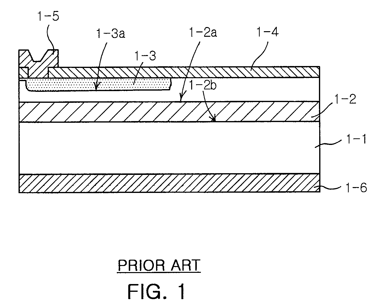
In this case, damages in a silicon lattice occur due to high energy ion implantation, which cause a current leakage, thereby deteriorating breakdown voltage characteristics.
Accordingly, since a conventional silicon APD uses a double side process, it is difficult to manage the conventional APD.
In the high energy ion implantation process, damages in a silicon lattice is caused, which are difficult to be adjusted.
For this, the wafer has to be turned upside down, which is troublesome.
Due to the double side process, it is difficult to manage conventional APDs.
Accordingly, when attaching a CMOS circuit to the APD, respective diodes thereof are formed separately from each other and connected to a circuit, which is troublesome.

Method used


Image

  • CMOS-based planar type silicon avalanche photo diode using silicon epitaxial layer and method of manufacturing the same
  • CMOS-based planar type silicon avalanche photo diode using silicon epitaxial layer and method of manufacturing the same
  • CMOS-based planar type silicon avalanche photo diode using silicon epitaxial layer and method of manufacturing the same

Examples


Embodiment Construction

[0032]Exemplary embodiments of the present invention will now be described in detail with reference to the accompanying drawings.

[0033]Only, in describing operations of the exemplary embodiments in detail, when it is considered that a detailed description on related well-known functions or constitutions may make essential points of the present invention be unclear, the detailed description will be omitted.

[0034]In the drawings, the same reference numerals are used throughout to designate the same or similar components.

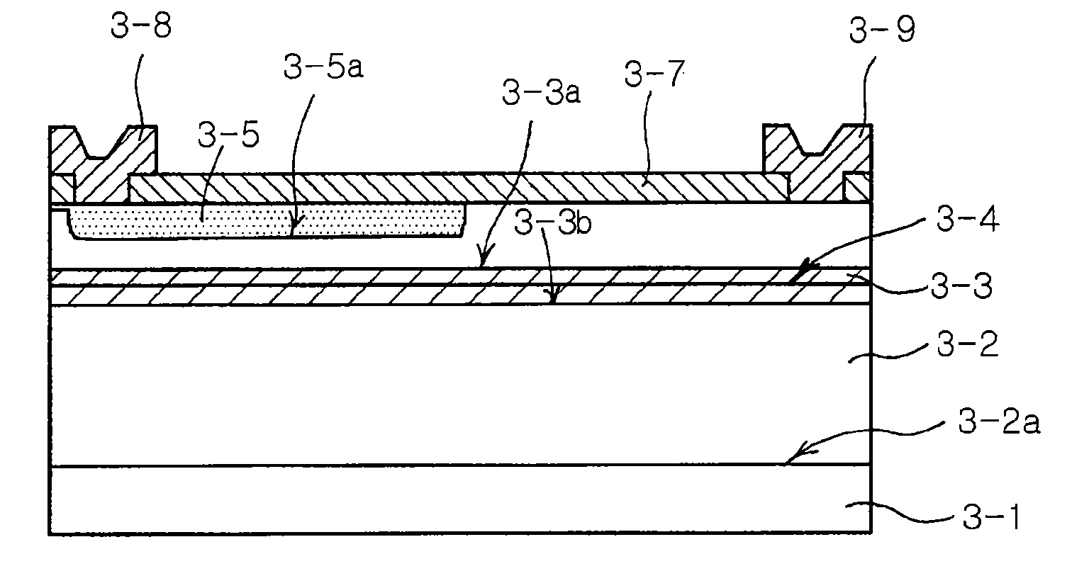
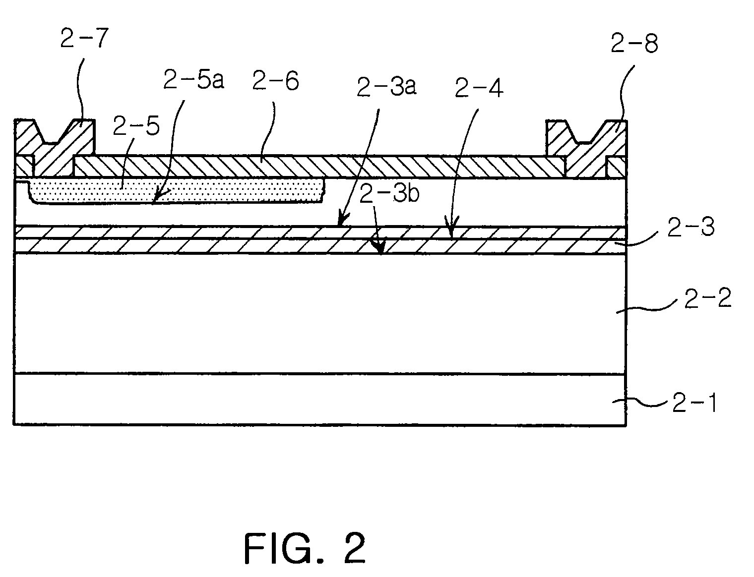
[0035]A configuration and a complementary metal-oxide semiconductor (CMOS)-based planar type avalanche photo diode (APD) using a silicon epitaxial layer 2-4 and a method of manufacturing the APD, according to an exemplary embodiment of the present invention, will be described with reference to the attached drawings.

[0036]FIG. 2 is a cross-sectional view illustrating the APD according to an exemplary embodiment of the present invention.

[0037]The APD includes a substrate...


PUM


Abstract

A complementary metal-oxide semiconductor (CMOS)-based planar type avalanche photo diode (APD) using a silicon epitaxial layer and a method of manufacturing the APD, the photo diode including: a substrate; a well layer of a first conductivity type formed in the substrate; an avalanche embedded junction formed in the well layer of the first conductivity type by low energy ion implantation; the silicon epitaxial layer formed in the avalanche embedded junction; a doping area of a second conductivity type opposite to the first conductive type, formed from a portion of a surface of the well layer of the first conductivity type in the avalanche embedded junction and forming a p-n junction; positive and negative electrodes formed on the doping area of the second conductivity type and the well layer of the first conductivity type separated from the doping area of the second conductivity type, respectively; and an oxide layer formed on an overall surface excluding a window where the positive and negative electrodes are formed.

Description

CROSS-REFERENCE TO RELATED APPLICATIONS[0001]This application claims the priority of Korean Patent Application No. 10-2007-0128278 filed on Dec. 11, 2007, in the Korean Intellectual Property Office, the disclosure of which is incorporated herein by reference.BACKGROUND OF THE INVENTION[0002]1. Field of the Invention[0003]The present invention relates to a complementary metal-oxide semiconductor (CMOS)-based planar type avalanche photo diode (APD) and a method of manufacturing the same.[0004]2. Description of the Related Art[0005]An avalanche photo diode (APD) indicates a diode using an avalanche phenomenon, in which a layer forming a high electric field in a middle of the diode is required. The layer is called as an embedded junction.[0006]In a conventional APD, the embedded junction is formed by high energy ion implantation. In this case, damages in a silicon lattice occur due to high energy ion implantation, which cause a current leakage, thereby deteriorating breakdown voltage ch...

Claims


Application Information

Patent Timeline
Patent Type & Authority Patents(United States)
IPC IPC(8): H01L31/062
CPCH01L31/107
Inventor YOON, YONG SUNPARK, KUN SIKPARK, JONG MOONKIM, BO WOOKANG, JIN YEONG
Owner ELECTRONICS & TELECOMM RES INST
Learn More