
Semiconductor device having an increased area of one of the opposing electrode parts for preventing generation of unconnected positions the electrodes on the bonded wafers

a technology of opposing electrodes and electrodes, which is applied in the direction of semiconductor devices, semiconductor/solid-state device details, electrical apparatus, etc., can solve the problems of increasing the complexity of wiring on the wafer, and increasing the area of one of the opposing electrode parts. , to achieve the effect of high reliability of electrical connection

Inactive Publication Date: 2011-07-26
HONDA MOTOR CO LTD
View PDF4 Cites 16 Cited by
  • Summary
  • Abstract
  • Description
  • Claims
  • Application Information

AI Technical Summary

Benefits of technology

The present invention is a semiconductor device that includes a first wafer and a second wafer bonded together. The device has multiple electrical signal connection parts on both wafers that are insulated from each other. The shape of the second electrical signal connection parts is larger than the shape of a positioning margin face, which ensures reliable alignment of the electrode parts on the wafers and prevents unconnected portions between them. The semiconductor device can be configured with different positioning margin dimensions and can be thinned wafers or wafers with penetrating wiring parts or bumps. The technical effect of the invention is to achieve reliable electrical connection between the electrode parts on the wafers and prevent unconnected portions between them, even in cases of misalignment or warpage during manufacturing.

Problems solved by technology

However, there is a problem in a conventional semiconductor device in which a plurality of wafers are bonded together, in that there may be positional deviation among some of the electrode parts to be connected on opposite sides of the wafers, leading to portions where electrodes are unconnected.
This problem becomes more noticeable when the wafers are made larger and thinner, and when the electrode parts are miniaturized and multi-layered wirings on the wafers are made more complex.

Method used


Image

  • Semiconductor device having an increased area of one of the opposing electrode parts for preventing generation of unconnected positions the electrodes on the bonded wafers
  • Semiconductor device having an increased area of one of the opposing electrode parts for preventing generation of unconnected positions the electrodes on the bonded wafers
  • Semiconductor device having an increased area of one of the opposing electrode parts for preventing generation of unconnected positions the electrodes on the bonded wafers

Examples


first embodiment

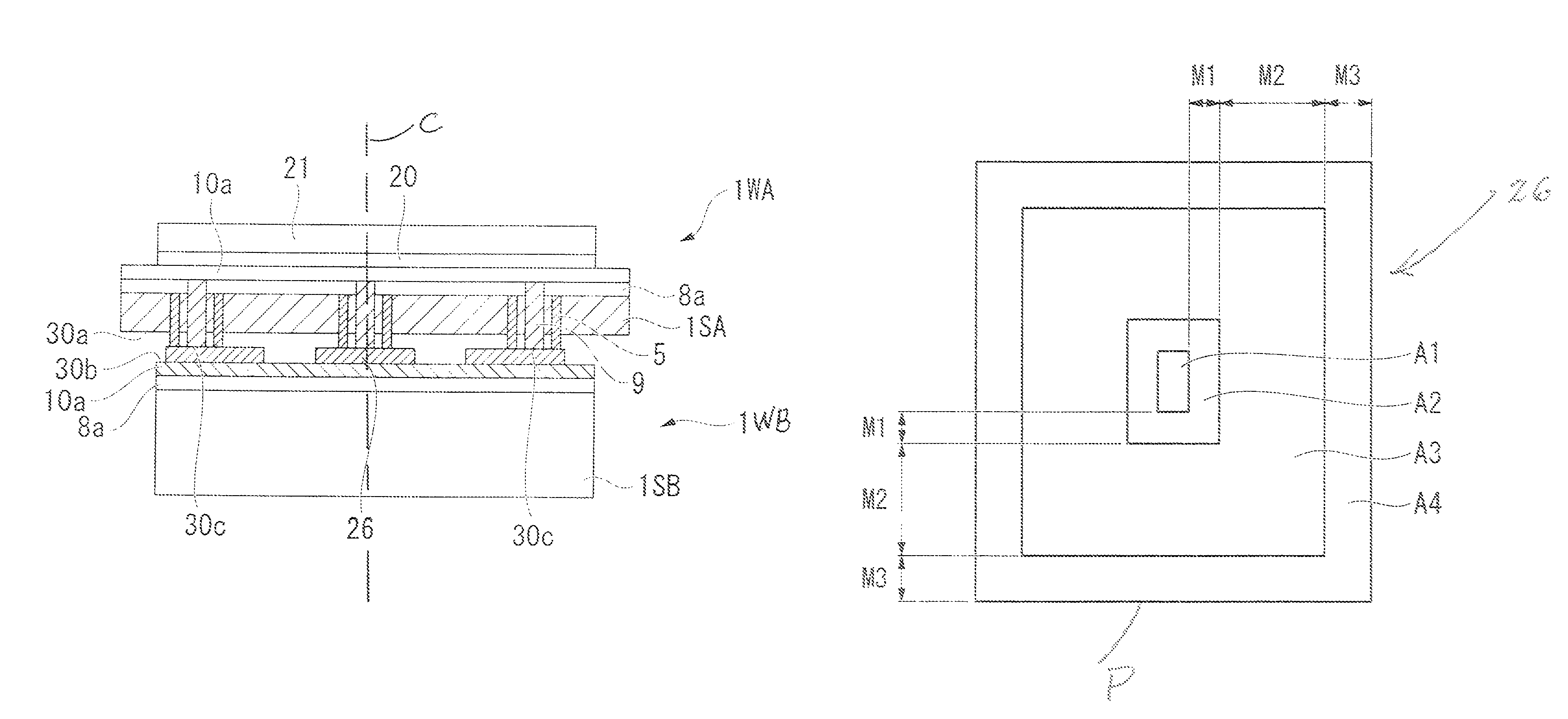
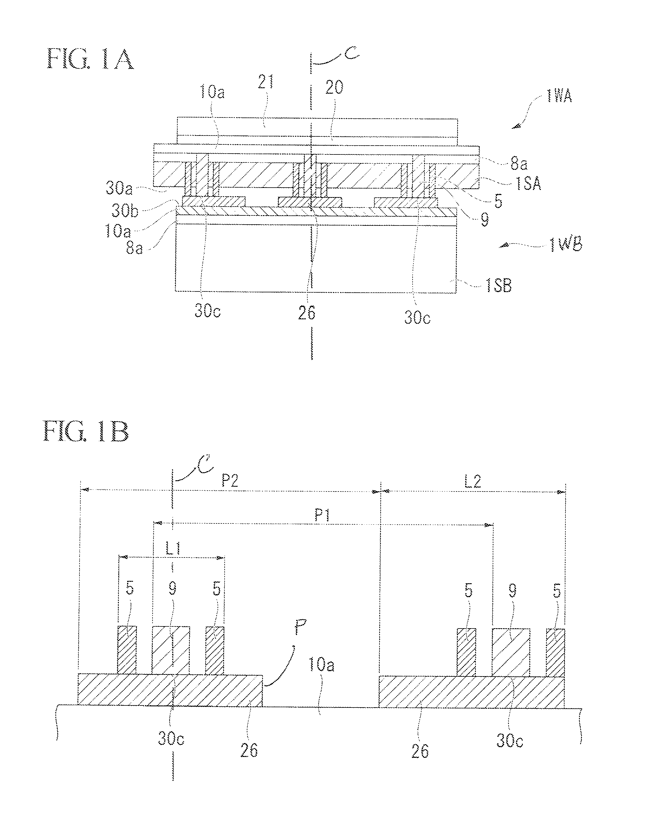
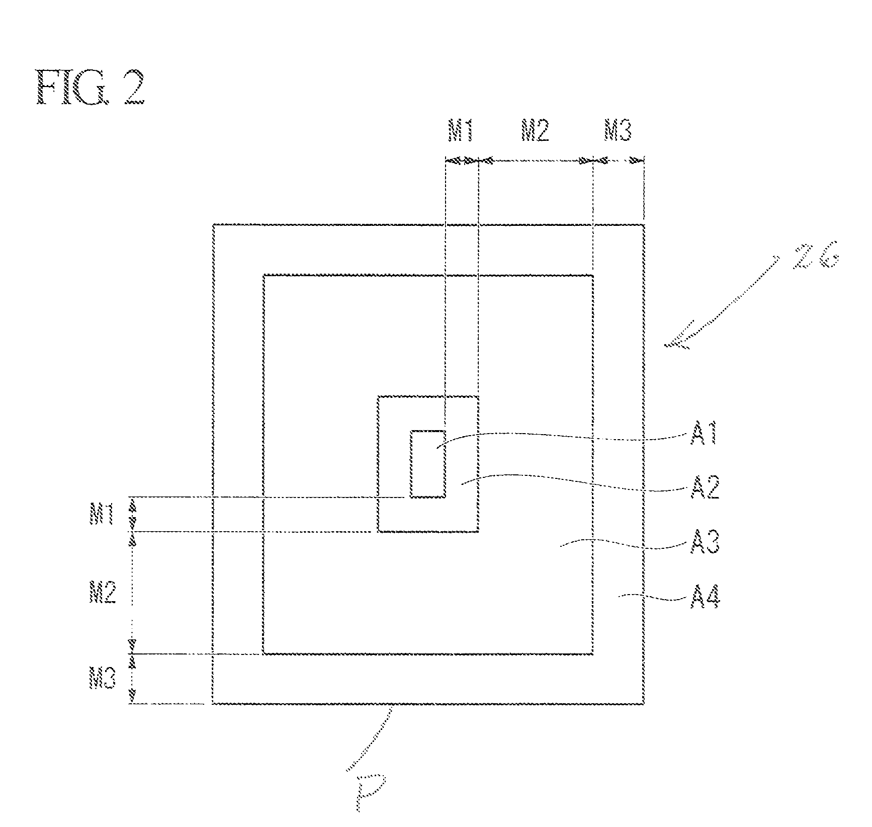
[0069]FIGS. 1A to 20 are explanatory views of a first embodiment of the semiconductor device of the invention. FIG. 19 is a cross-sectional view of primary parts of the semiconductor device of this embodiment. FIGS. 1A and 1B are enlarged cross-sectional schematic views of a part of the semiconductor device of this embodiment. FIG. 2 is an explanatory plan view of the relationship between the size of a penetrating wiring part and a bump in the semiconductor device of this embodiment. FIGS. 3 to 18 are explanatory views of manufacturing processes of the semiconductor device of this embodiment. FIG. 20 is an explanatory flowchart of a manufacturing process of the semiconductor device of this embodiment.

[0070]In the semiconductor device of the embodiment shown in FIG. 19, an upper wafer 1WA and a lower wafer 1WB are bonded together. The wafer 1WA and the wafer 1WB are manufactured by processing substrates 1SA and 1SB. A bonding surface 30a of the upper wafer 1WA is arranged opposite th...

second embodiment

[0139]FIGS. 22 to 42 are explanatory views of a semiconductor device according to a second embodiment. FIG. 41 is a cross-sectional view of primary parts of an example of the semiconductor device of the invention, FIG. 22 is an enlarged schematic view of one part of the semiconductor device shown in FIG. 41, and FIG. 23 is an explanatory plan view of the relationship between the size of a penetrating wiring part and a bump in the semiconductor device shown in FIG. 22. FIGS. 24 to 40 are explanatory views of processes of manufacturing the semiconductor device shown in FIG. 41, and FIG. 42 is an explanatory flowchart of processes of manufacturing the semiconductor device shown in FIG. 41.

[0140]In the semiconductor device of the embodiment shown in FIGS. 22 to 42, like members to those in FIG. 18 are designated with like reference numerals, and are not repetitiously explained.

[0141]The semiconductor device of the embodiment shown in FIG. 41 differs from the semiconductor device shown i...

experimental example

[0191]Using a silicon substrate having a diameter of 200 mm (eight inches) and a thickness of 30 μm, an upper wafer having penetrating isolation parts and penetrating wiring parts formed thereon was made in the same manner as the upper wafer 1WA of the semiconductor device shown in FIG. 19.

[0192]The penetrating wiring part on the upper wafer 1WA includes two wiring parts made of tungsten, whose cross-sectional shape is that of a rectangle having a vertical dimension of 5.6 μm and a horizontal dimension of 1.5 μm, these being arranged in parallel with an interval of 2.6 μm between them. The length of the penetrating protrusions in the thickness direction of the wafer 1WA was 40 μm. In the design of the pre-processed substrate, the pitch for arranging the penetrating wiring parts was set at 50 μm. The penetrating isolation parts are square frames having external length and width of 13.4 μm.

[0193]For the upper wafer 1WA thus obtained, a positioning margin was determined (i.e. the diffe...


PUM


Abstract

In this semiconductor device, connection parts between wafers are electrically insulated from each other, and a junction face shape of second electrical signal connection parts is larger than the shape of a positioning margin face that is formed by an outer shape when the periphery of a minimum junction face, which has half the area of a junction area of the first electrical signal connection part, is enclosed by a same width dimension as a positioning margin dimension between the first wafer and the second wafer.

Description

[0001]Priority is claimed on U.S. Provisional Application No. 60 / 957,792, filed Aug. 24, 2007, the content of which are incorporated herein by reference.BACKGROUND OF THE INVENTION[0002]1. Field of the Invention[0003]The present invention relates to a semiconductor device.[0004]2. Description of Related Art[0005]Conventionally, a three-dimensional semiconductor integrated circuit device has been known having a configuration wherein two or more wafers are stacked and electrically connected with penetrating wiring.[0006]For example, Japanese Unexamined Patent Application, First Publication No. H11-261000 discloses a semiconductor device obtained by the following manufacturing method. After making a trench (i.e., a deep groove) in one of the wafers to be stacked and thermally-oxidizing an inner part of the trench, Poly-Si is buried in the trench as a conductor to form a penetrating wiring. The wafer thickness is reduced until the penetrating wiring is exposed, and backside bumps are fo...

Claims


Application Information

Patent Timeline
Patent Type & Authority Patents(United States)
IPC IPC(8): H01L23/48H01L23/52H01L29/40
CPCH01L21/6835H01L24/17H01L21/76898H01L23/481H01L24/12H01L24/16H01L24/83H01L24/90H01L25/0657H01L25/50H01L21/563H01L2924/1305H01L2924/1306H01L2924/07802H01L2224/171H01L2221/68372H01L2224/13099H01L2224/838H01L2225/06513H01L2225/06541H01L2924/01002H01L2924/01005H01L2924/01013H01L2924/01015H01L2924/01022H01L2924/01029H01L2924/01074H01L2924/01078H01L2924/01082H01L2924/01088H01L2924/04941H01L2924/13091H01L2924/14H01L2924/19041H01L2924/19042H01L2924/19043H01L2924/01006H01L2924/01019H01L2924/01033H01L2924/01037H01L2224/13078H01L2924/00H01L2224/131H01L2224/05085H01L2224/05022H01L2224/05001H01L2224/05572H01L2224/05124H01L2224/05147H01L2224/05184H01L2224/05684H01L24/81H01L2224/10126H01L2224/10135H01L2224/10145H01L24/13H01L2924/00014
Inventor MAEBASHI, TAKANORIMIYAKAWA, NOBUAKI
Owner HONDA MOTOR CO LTD
Learn More