MOSFET parametric amplifier
a parametric amplifier and amplifier technology, applied in the field of circuits, can solve the problems of low power, low noise, and large signal amplification, and achieve the effect of low power
- Summary
- Abstract
- Description
- Claims
- Application Information
AI Technical Summary
Benefits of technology
Problems solved by technology
Method used
Image
Examples
fourth embodiment
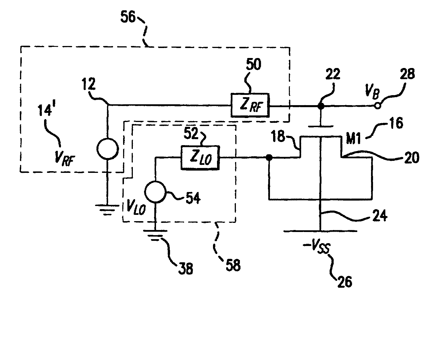
[0067]FIG. 17 depicts a fourth embodiment according to the present invention. In this embodiment, which is similar to FIG. 10, a capacitor 45′ may be connected in parallel with the gate terminal 22. Preferably a variable capacitor may be used. This may be used to control the gain by controlling the load.
[0068]In many applications like pipeline ADCs (analog-to-digital converters) a gain of 2 is required. The parametric amplifier has a maximum gain larger than 2. Variable gains may be attained by adjusting the voltage to which the source is boosted or by adjusting the capacitance 45′ that the parametric amplifier is loaded with. In a alternate embodiment, a parametric amplifier may be put in a negative feedback loop to adjust the gain to 2, by varying either or both (the pulling voltage and / or the capacitor value) of these parameters. This may require the use of other components, such as op amps and filters to obtain sufficient loop gain.
[0069]One parametric amplifier may also be used...
sixth embodiment
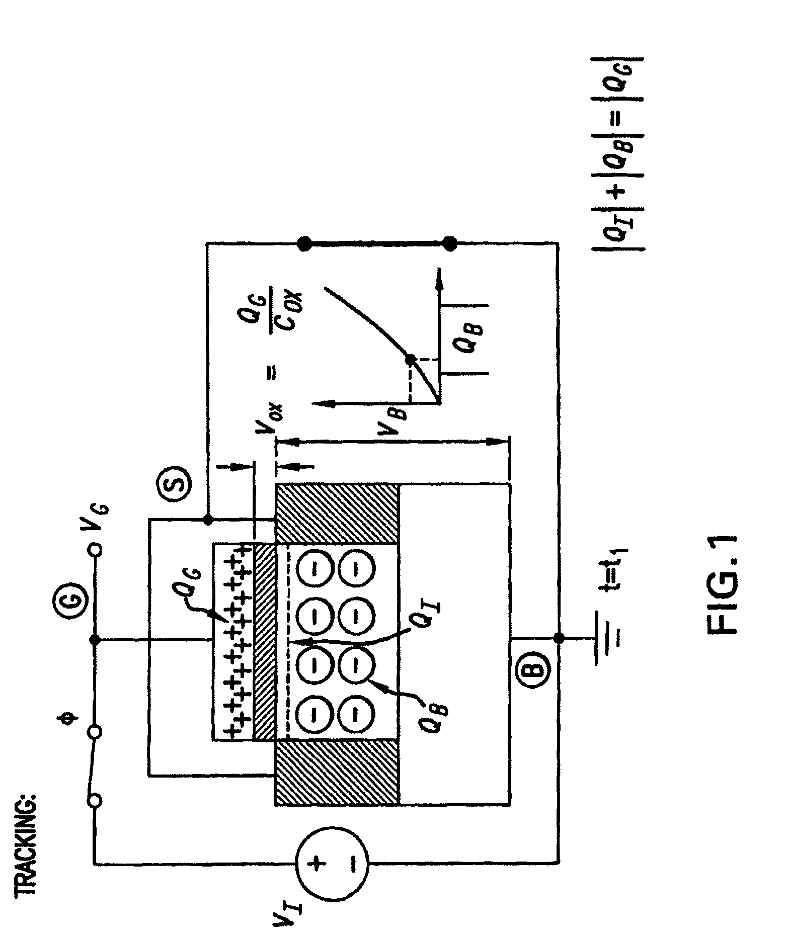
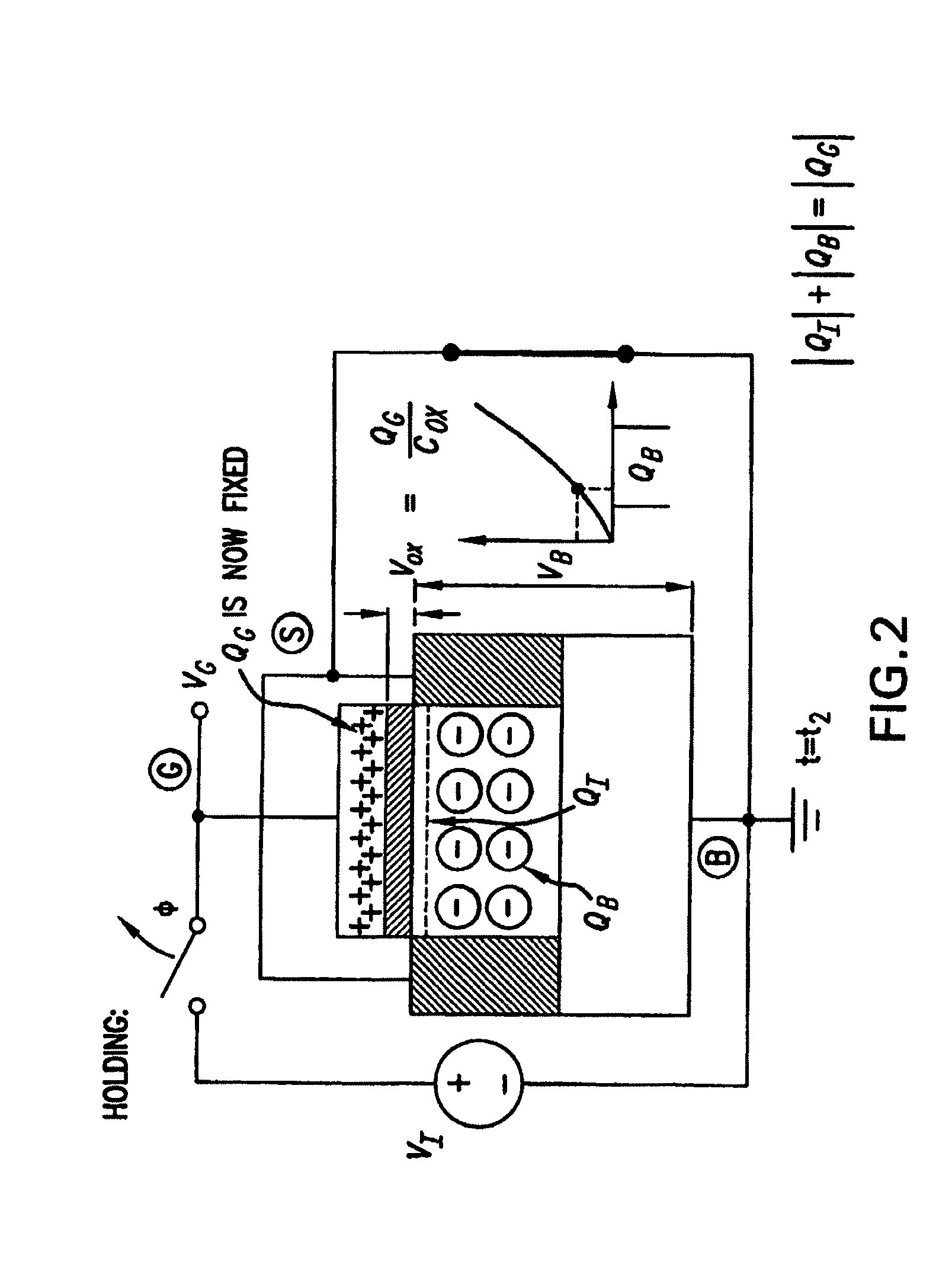
[0080]The requirement of a small gain for a sampled input, at a high frequency using low power is met well by the MOSFET parametric amplifier. The topology of this comparator is shown in a sixth embodiment according to the present invention in FIG. 22. In phase φ1 the input may be sampled at the gate 2230, 2240 of the MOSFET's 2210, 2220 as well as at the input of the latch. The source and drain of MOSFET's 2210, 2220 may be connected to ground 2250 at that time. In the next non-overlapping phase φ2, the source and drain of the MOSFET's 2210, 2220 may be pulled up to Vdd. This may pull in all the inversion charge from under the gate depleting the device. The results in a boosting of the gate voltage, and in differential operation in a gain.
[0081]At the end of the sampling phase, the input voltage may already be available at the gate, which is also the input of the latch. The time taken by the amplifier to amplify may be the sum of the time it takes for the drain, source terminals to...
PUM
 Abstract
Description
Claims
Application Information
 - R&D
- Intellectual Property
- Life Sciences
- Materials
- Tech Scout
- Unparalleled Data Quality
- Higher Quality Content
- 60% Fewer Hallucinations
Browse by: Latest US Patents, China's latest patents, Technical Efficacy Thesaurus, Application Domain, Technology Topic, Popular Technical Reports.
© 2025 PatSnap. All rights reserved.Legal|Privacy policy|Modern Slavery Act Transparency Statement|Sitemap|About US| Contact US: help@patsnap.com


