Card type information device and method for manufacturing same
a technology of information device and card, which is applied in the direction of loop antenna with ferromagnetic core, instrument, and device details, etc., can solve the problem of difficult placement of antenna along the end face, and achieve the effect of reducing cos
- Summary
- Abstract
- Description
- Claims
- Application Information
AI Technical Summary
Benefits of technology
Problems solved by technology
Method used
Image
Examples
first exemplary embodiment
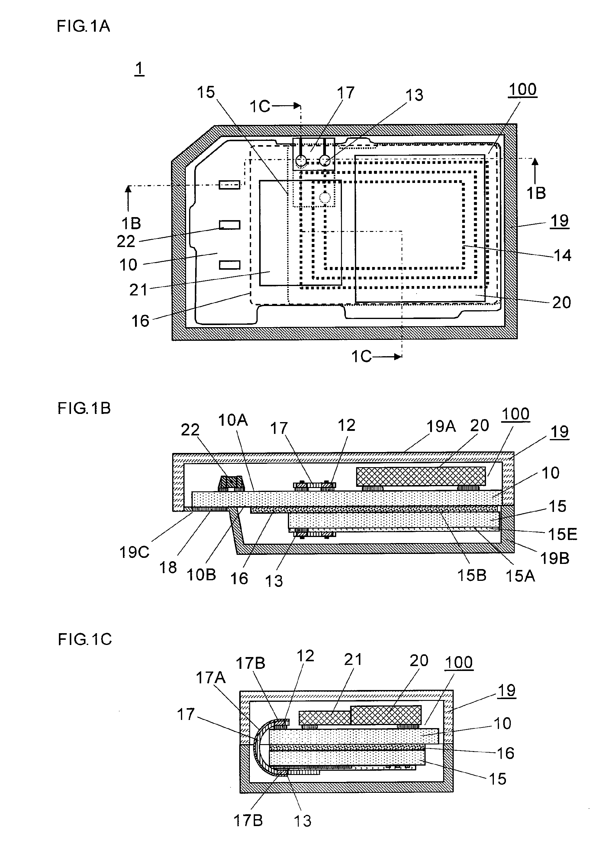
[0101]FIG. 1A shows a plan view schematically illustrates a structure of a card type information device (hereinafter referred to as SD memory card) in accordance with the first exemplary embodiment of the present invention. FIG. 1B shows a sectional view cut along line 1B-1B in FIG. 1A. FIG. 1C shows a sectional view cut along line 1C-1C in FIG. 1A. In FIG. 1A, an upper section of the housing is omitted in order to show the interior structure more clearly.
[0102]As shown in FIG. 1A, SD memory card 1 has outer dimensions of 24 mm×32 mm×2.1 mm specified by the industry standard and includes housing 19 made of a polymer alloy of polycarbonate and ABS resin. Housing 19 accommodates the following elements:[0103]wiring board 10 including a wiring pattern (not shown) having multiple electronic components, e.g. semiconductor memory elements, and control circuit elements mounted on first face 10A of wiring board 10, and antenna connecting electrode 12; and[0104]antenna board 15 of which first...
second exemplary embodiment
[0133]FIG. 6A shows a plan view schematically illustrates a structure of an SD memory card in accordance with the second exemplary embodiment of the present invention. FIG. 6B shows a schematic sectional view cut along line 6B-6B shown in FIG. 6A, and FIG. 6C shows a schematic sectional view cut along line 6C-6C shown in FIG. 6A. In FIG. 6A, an upper section of the housing is omitted in order to clearly show the interior structure. In FIG. 6A-FIG. 6C, similar elements to those in FIG. 1A-FIG. 1C have the same reference marks as those in FIG. 1A-FIG. 1C.
[0134]As shown in FIG. 6A-FIG. 6C, SD memory card 2 in accordance with the second exemplary embodiment differs from SD memory card 1 shown in FIG. 1A-FIG. 1C in the following point: Wiring board 10 and antenna board 15 of SD memory card 2 have a curved end face at least at a section where both wiring board 10 and antenna board 15 are coupled together through flexible wiring board 17.
[0135]To be more specific, as shown in FIG. 6C, SD m...
third exemplary embodiment
[0150]FIG. 10A shows a plan view schematically illustrates a structure of an SD memory card in accordance with the third exemplary embodiment of the present invention. FIG. 10B shows a schematic sectional view cut along line 10B-10B shown in FIG. 10A, and FIG. 10C shows a schematic sectional view cut along line 10C-10C shown in FIG. 10A. In FIG. 10A, an upper section of the housing is omitted in order to clearly show the interior structure. In FIG. 10A-FIG. 10C, similar elements to those in FIG. 1A-FIG. 1C have the same reference marks as those in FIG. 1A-FIG. 1C.
[0151]As shown in FIG. 10A-FIG. 10C, wiring board 10 differs from that shown in FIG. 1A-FIG. 1C in having no external connecting terminal, and the other structures remain unchanged from those in FIG. 1A-FIG. 1C. As shown in FIG. 10A-FIG. 10C, solid circuit module 400 of SD memory card 4 has no external connecting terminal at wiring board 40 for connecting to an external device through housing 49, so that no hole is needed t...
PUM
| Property | Measurement | Unit |
|---|---|---|
| thickness | aaaaa | aaaaa |
| thickness | aaaaa | aaaaa |
| thickness | aaaaa | aaaaa |
Abstract
Description
Claims
Application Information
 - R&D
- Intellectual Property
- Life Sciences
- Materials
- Tech Scout
- Unparalleled Data Quality
- Higher Quality Content
- 60% Fewer Hallucinations
Browse by: Latest US Patents, China's latest patents, Technical Efficacy Thesaurus, Application Domain, Technology Topic, Popular Technical Reports.
© 2025 PatSnap. All rights reserved.Legal|Privacy policy|Modern Slavery Act Transparency Statement|Sitemap|About US| Contact US: help@patsnap.com


