Light emitting diode chip
a diode chip and light-emitting technology, applied in the field of semiconductor/solid-state device manufacturing, semiconductor devices, electrical apparatus, etc., can solve the problems of quality degradation of epitaxy, reduce voltage drop, low operation voltage, and reduce leakage current
- Summary
- Abstract
- Description
- Claims
- Application Information
AI Technical Summary
Benefits of technology
Problems solved by technology
Method used
Image
Examples
first embodiment
The First Embodiment
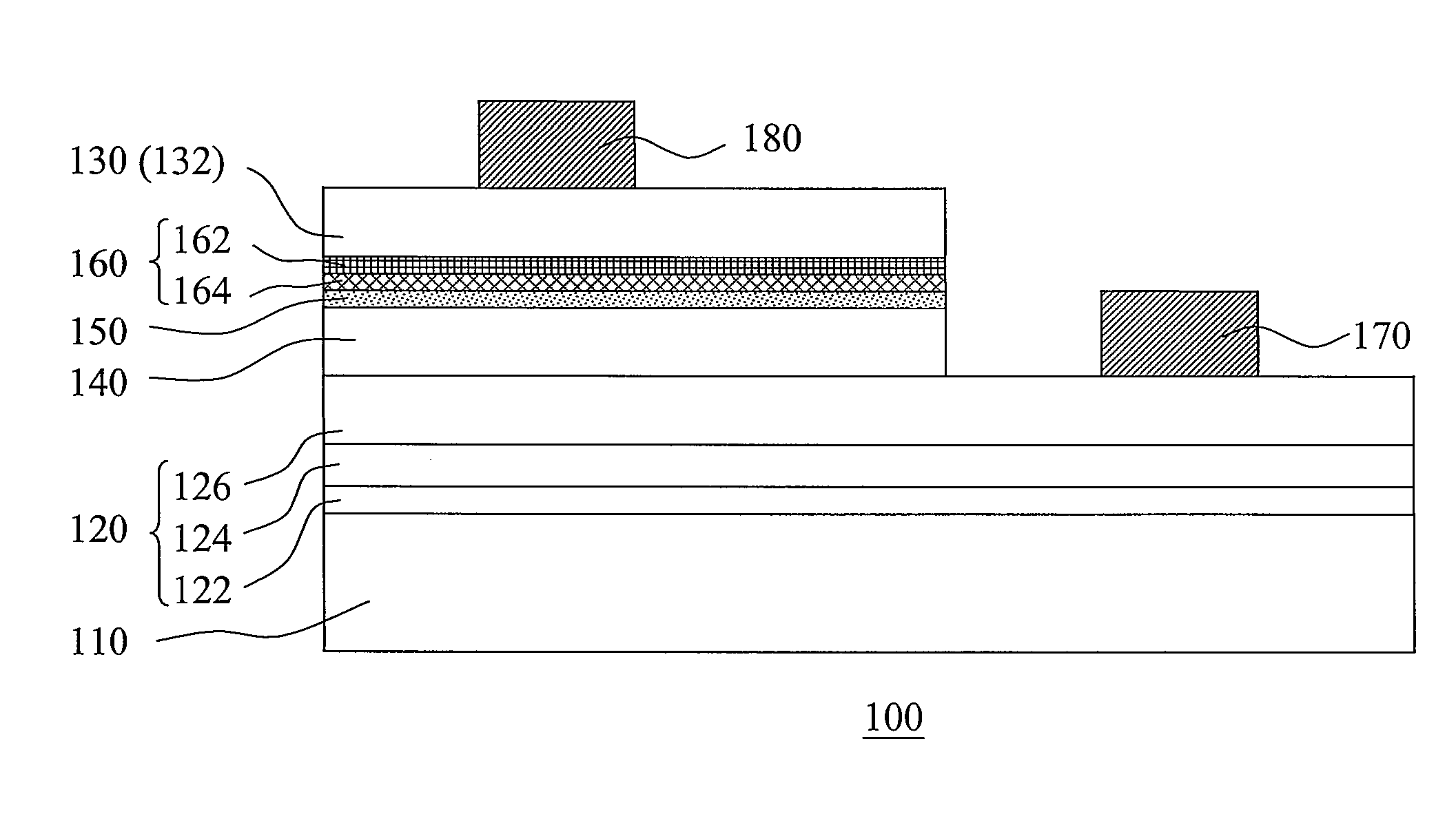
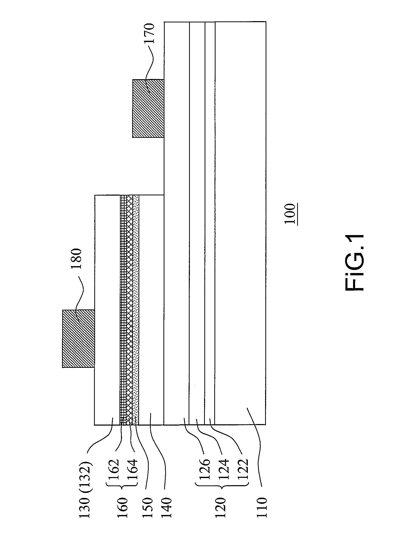
[0028]FIG. 1 is a cross-sectional schematic view of an LED chip according to a first embodiment of the present invention. Referring to FIG. 1, an LED chip 100 of the present invention comprises a chip 110, a first type doped semiconductor layer 120, a second type doped semiconductor layer 130, a light emitting layer 140, an Indium-doped AlxGa1-xN based material layer (0≦x150, a tunneling junction layer 160, a first electrode 170, and a second electrode 180. The first type doped semiconductor layer 120 is disposed on the substrate 110, and the second type doped semiconductor layer 130 is disposed above the first type doped semiconductor layer 110. The light emitting layer 140 is disposed between the first type doped semiconductor layer 120 and the second type doped semiconductor layer 130. In addition, the first electrode 170 is disposed on the first type doped semiconductor layer 110, and the second electrode 180 is disposed on the second type doped semiconductor...
second embodiment
The Second Embodiment
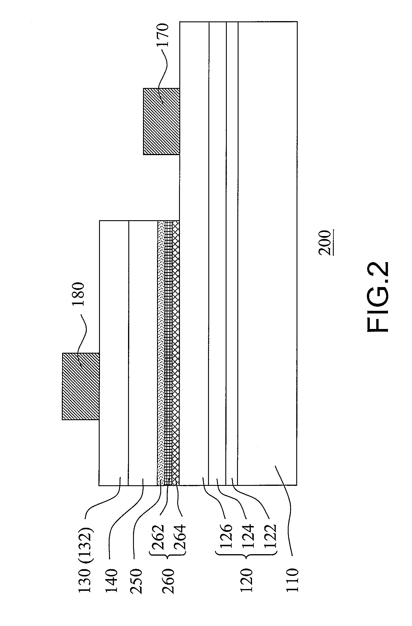
[0041]FIG. 2 is a cross-sectional view of the LED chip according to a second embodiment of the present invention. Referring to FIG. 2, the LED chip 200 of the second embodiment is similar to the LED chip 100 (shown in FIG. 1) of the first embodiment; the difference is that the disposition of the Indium-doped AlxGa1-xN based material layer (0≦x250 and the tunneling junction layer 260 are different. In this embodiment, the Indium-doped AlxGa1-xN based material layer 250 is disposed on the lower surface of the light emitting layer 140, and the tunneling junction layer 260 is disposed between the Indium-doped AlxGa1-xN based material layer 250 and the fist type doped semiconductor layer 120. Also, the tunneling junction layer 260 comprises a first type AlxGa1-xN based material layer (0≦x262 and a second type AlxGa1-xN based material layer (0≦x264, wherein the first type AlxGa1-xN based material layer 262 is disposed between the Indium-doped AlxGa1-xN based material ...
fourth embodiments
The Third and Fourth Embodiments
[0045]FIG. 3 is a cross-sectional view of the LED chip according to the third embodiment of the present invention, and FIG. 4 is a cross-sectional view of the LED chip according to a fourth embodiment of the present invention. Referring to FIG. 3, the LED chip 300 of the third embodiment is similar to the LED chip 100 (shown in FIG. 1) of the first embodiment; the difference is that the first type AlxGa1-xN based material layer 362 of the tunneling junction layer 360 is a p-type AlxGa1-xN based material layer, and the second type AlxGa1-xN based material layer 364 is an n-type AlxGa1-xN based material layer. Referring to FIG. 4, the LED chip 400 of the fourth embodiment is similar to the LED chip 200 of the second embodiment (shown in FIG. 2); the difference is that the first type AlxGa1-xN based material layer 462 of the tunneling junction layer 460 is a p-type AlxGa1-xN based material layer, and the second type AlxGa1-xN based material layer 464 is ...
PUM
 Abstract
Description
Claims
Application Information
 - R&D
- Intellectual Property
- Life Sciences
- Materials
- Tech Scout
- Unparalleled Data Quality
- Higher Quality Content
- 60% Fewer Hallucinations
Browse by: Latest US Patents, China's latest patents, Technical Efficacy Thesaurus, Application Domain, Technology Topic, Popular Technical Reports.
© 2025 PatSnap. All rights reserved.Legal|Privacy policy|Modern Slavery Act Transparency Statement|Sitemap|About US| Contact US: help@patsnap.com


