
Top-emission organic light-emitting display device

a display device and organic technology, applied in thermoelectric devices, instruments, building rescue and other directions, can solve problems such as degrading the quality of screens, and achieve the effect of improving non-uniform brightness

Active Publication Date: 2010-06-22
SAMSUNG DISPLAY CO LTD
View PDF27 Cites 8 Cited by
  • Summary
  • Abstract
  • Description
  • Claims
  • Application Information

AI Technical Summary

Benefits of technology

The solution achieves stable and uniform contact resistance, enhancing the brightness uniformity between pixels and improving the overall quality of the display by preventing corrosion and maintaining low contact resistance.

Problems solved by technology

The increase in the dispersion of the contact resistance in the substrate causes non-uniformity in brightness between pixels when operating the top-emission organic light-emitting display device, thereby greatly degrading the quality of a screen.

Method used


Image

  • Top-emission organic light-emitting display device
  • Top-emission organic light-emitting display device
  • Top-emission organic light-emitting display device

Examples


experimental example

[0079]The contact resistance of the top-emission organic light-emitting display devices obtained from the fabrication example and the comparative example was measured, and their surface states were observed using a microscope. This result is shown in FIGS. 9 to 12.

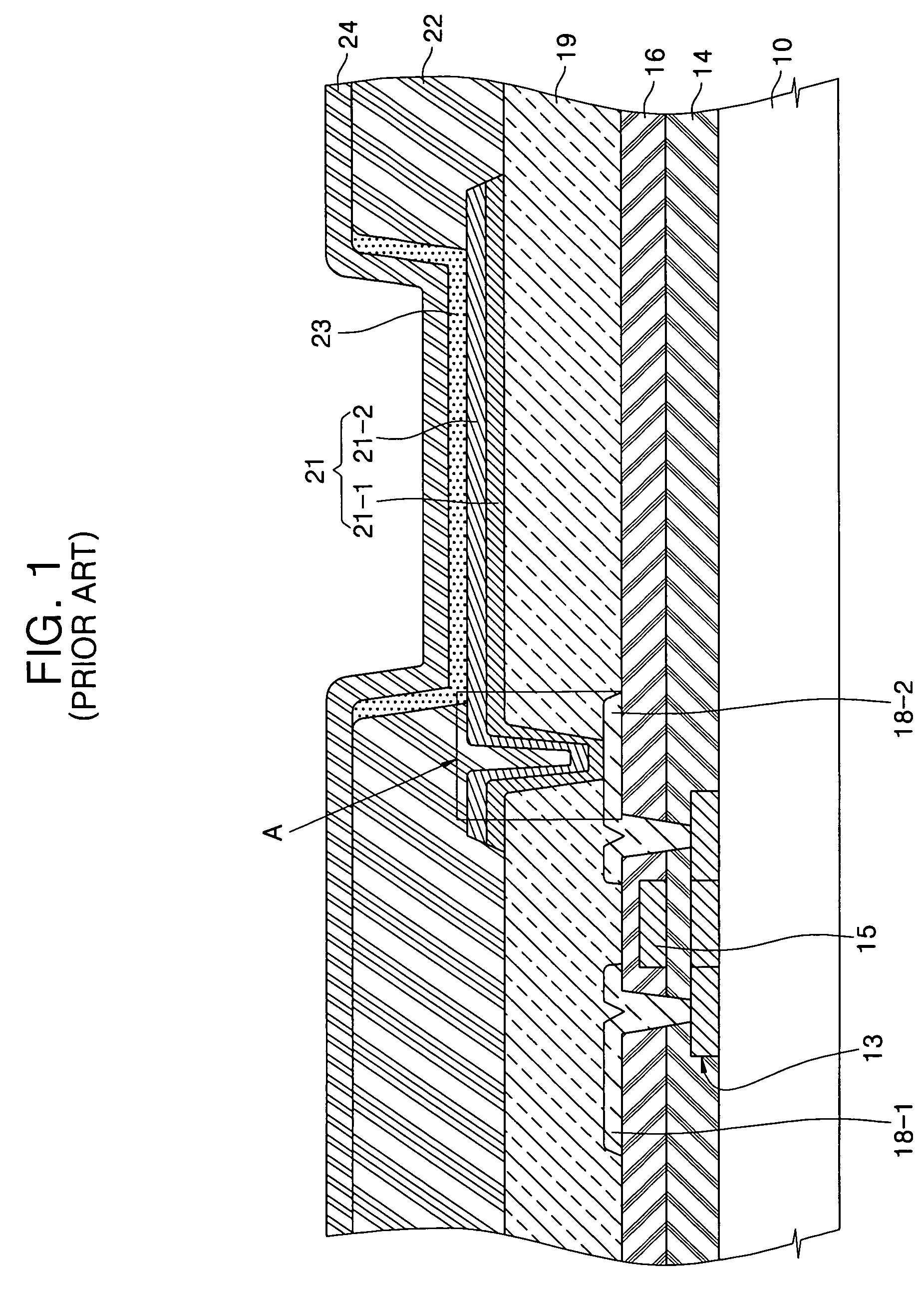
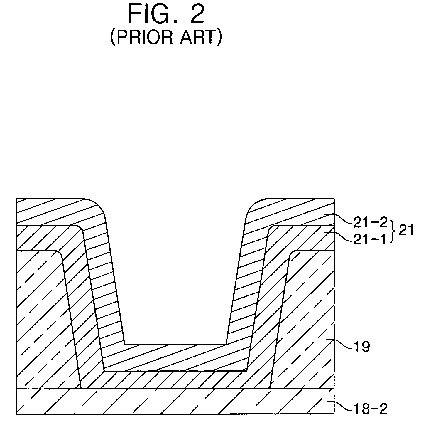
[0080]FIG. 9 is a graph obtained by measuring the contact resistance in the interface between the drain electrode and the first electrode (MoW and ITO) of the top-emission organic light-emitting display device obtained in the fabrication example. FIG. 10 is a graph obtained by measuring the contact resistance in the interfaces between the drain electrode, the reflective layer and the first electrode (MoW, AlNd and ITO) of the top-emission organic light-emitting display device obtained in the comparative example.

[0081]Referring to FIG. 9, numerical values of the contact resistance measured in several regions of the organic light-emitting display device are substantially similar to one another. This shows that the contact re...


PUM

PropertyMeasurementUnit
thickaaaaaaaaaa
transparentaaaaaaaaaa
insulatingaaaaaaaaaa

Abstract

An organic light-emitting display device and a method of fabricating the device are disclosed. The organic light-emitting display device includes a thin-film transistor positioned on a substrate that has a semiconductor layer, a gate electrode, and source and drain electrodes. A first electrode is positioned, which is connected to either the source electrode or drain electrode. A reflective layer, which is spaced apart from the source electrode or drain electrode, is positioned below the first electrode. An organic functional layer having at least an emission layer is positioned on the first electrode. A second electrode is positioned on the organic functional layer. The first electrode, the reflective layer, the organic functional layer, and the second electrode constitute an organic light-emitting diode.

Description

CROSS-REFERENCE TO RELATED APPLICATION[0001]This application claims priority to and the benefit of Korean Patent Application No. 2004-16608, filed Mar. 11, 2004, the disclosure of which is incorporated herein by reference in its entirety.BACKGROUND OF THE INVENTION[0002]1. Field of the Invention[0003]The present invention relates to a top-emission organic light-emitting display device in which the source or drain electrode of a thin-film transistor is in direct contact with a transparent electrode and a reflective layer is formed below the transparent electrode to be spaced from the source electrode and drain electrode.[0004]2. Description of the Related Art[0005]Typically, an organic light-emitting display (OLED) device has advantages over other flat panel displays in that it has a broader range of operable temperature, is stronger against impact or vibration, has a wider viewing angle, and has a faster response speed to provide clear moving pictures. Accordingly, the organic light...

Claims


Application Information

Patent Timeline
Patent Type & Authority Patents(United States)
IPC IPC(8): H01L29/786G02F1/1368H05B33/24H01L27/32H01L29/16H01L31/036H01L51/50H01L51/52H05B33/10H05B33/12H05B33/14H05B33/20H05B33/22H05B33/26H05B44/00
CPCH01L27/3248H01L51/5218H01L2251/5315H01L2227/323H01L51/5271H10K59/123H10K2102/3026H10K59/1201H10K59/878H10K59/80518A62B1/10A62B1/18H10K50/818H10K50/856
Inventor SEO, CHANG-SUPARK, MOON-HEEKANG, TAE-WOOKRYU, SEOUNG-YOONLEE, KWAN-HEE
Owner SAMSUNG DISPLAY CO LTD
Learn More