Vertical and trench type insulated gate MOS semiconductor device

a technology of insulating gate and semiconductor device, which is applied in the direction of semiconductor device, basic electric element, electrical apparatus, etc., can solve the problems of low turn-off capability, difficult to lower the on-voltage with a high current density, and inability to form the current path of the trench sidewall in the lateral direction. , to achieve the effect of enhancing the on-resistance and lowering the on-voltag

Active Publication Date: 2010-06-15
FUJI ELECTRIC CO LTD
View PDF11 Cites 4 Cited by
  • Summary
  • Abstract
  • Description
  • Claims
  • Application Information

AI Technical Summary

Benefits of technology

[0029]According to a third aspect of the invention, the vertical and trench type insulated gate MOS semiconductor device can be further adequately provided as a device in which the first conductivity type emitter region makes contact with the trench with a side the length of which is longer than the length of the contact region in the longitudinal direction of the trench.
[0082]According to the invention explained above, a vertical and trench type insulated gate MOS semiconductor device can be provided which can achieve lowered on-resistance and enhancement in turn-off capability.

Problems solved by technology

However, in the arrangement of the vertical trench type IGBT shown in FIG. 10, a problem is present in low turn-off capability.
When the device is applied under such a high current density condition, there is a problem with the arrangement of the related vertical and trench type IGBT shown in the above FIG. 10 in compatibility between the use at a high current density and reduction in an on-voltage.
However, only with the total emitter width widened according to the expression (1) for increasing the saturation current while keeping the arrangement of the vertical trench type IGBT shown in the above FIG. 10, it was found that the emitter region is made to come naturally closer to the end of the channel region in the longitudinal direction of the trench to make it impossible to form the current paths of the currents flowing on the sidewall of the trench in the lateral direction and to therefore make it difficult to lower the on-voltage with a high current density.

Method used


Image

  • Vertical and trench type insulated gate MOS semiconductor device
  • Vertical and trench type insulated gate MOS semiconductor device
  • Vertical and trench type insulated gate MOS semiconductor device

Examples


example 1

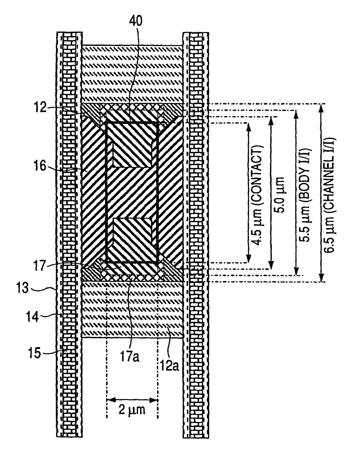
[0150]In the following, Example 1 of the vertical and trench type insulated gate MOS semiconductor device according to the invention will be explained with reference to FIG. 1 to FIG. 9, FIG. 13 and FIG. 14. In Example 1, a vertical IGBT with a breakdown voltage of 600V is taken as an example of a power vertical and trench type insulated gate MOS semiconductor device and its manufacturing process will be explained.

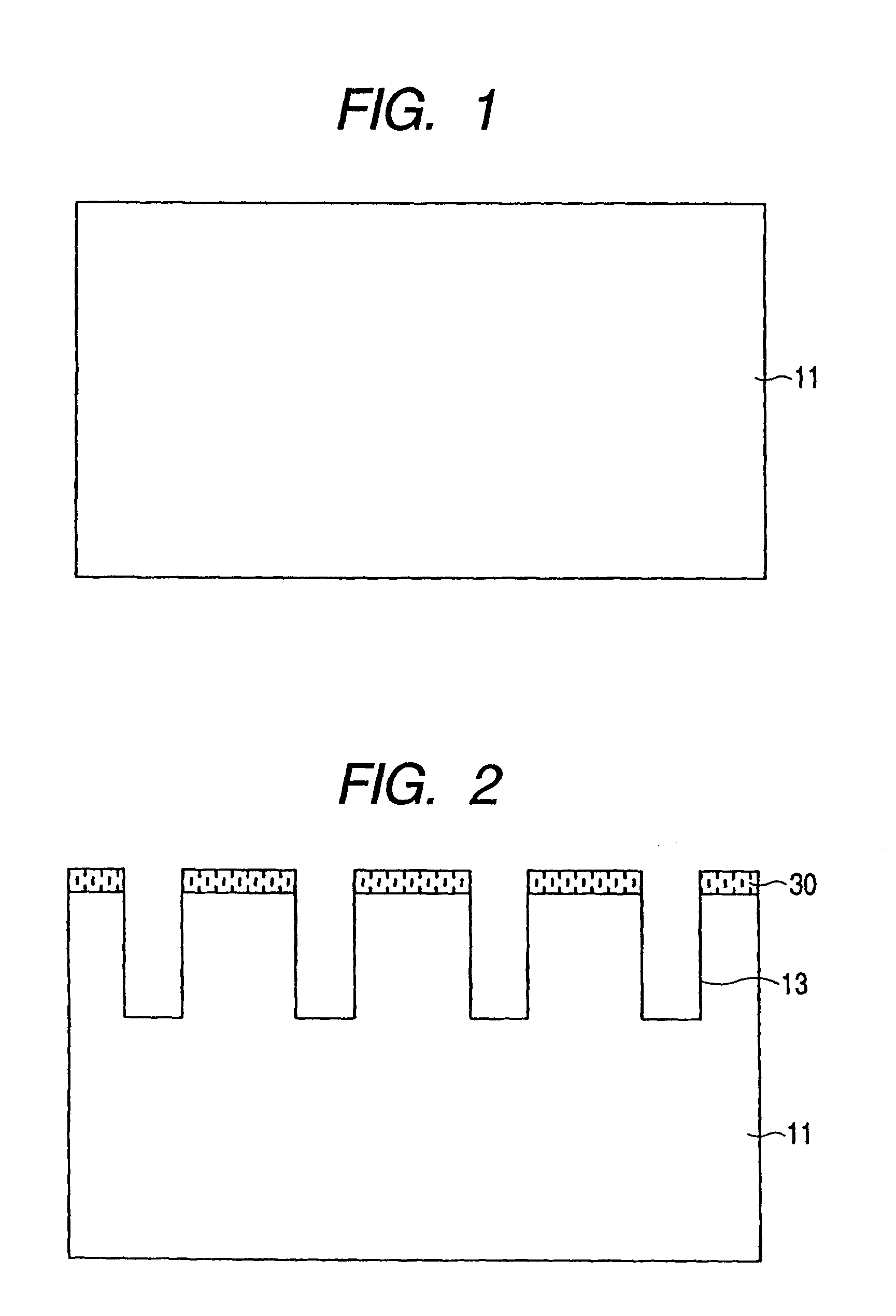
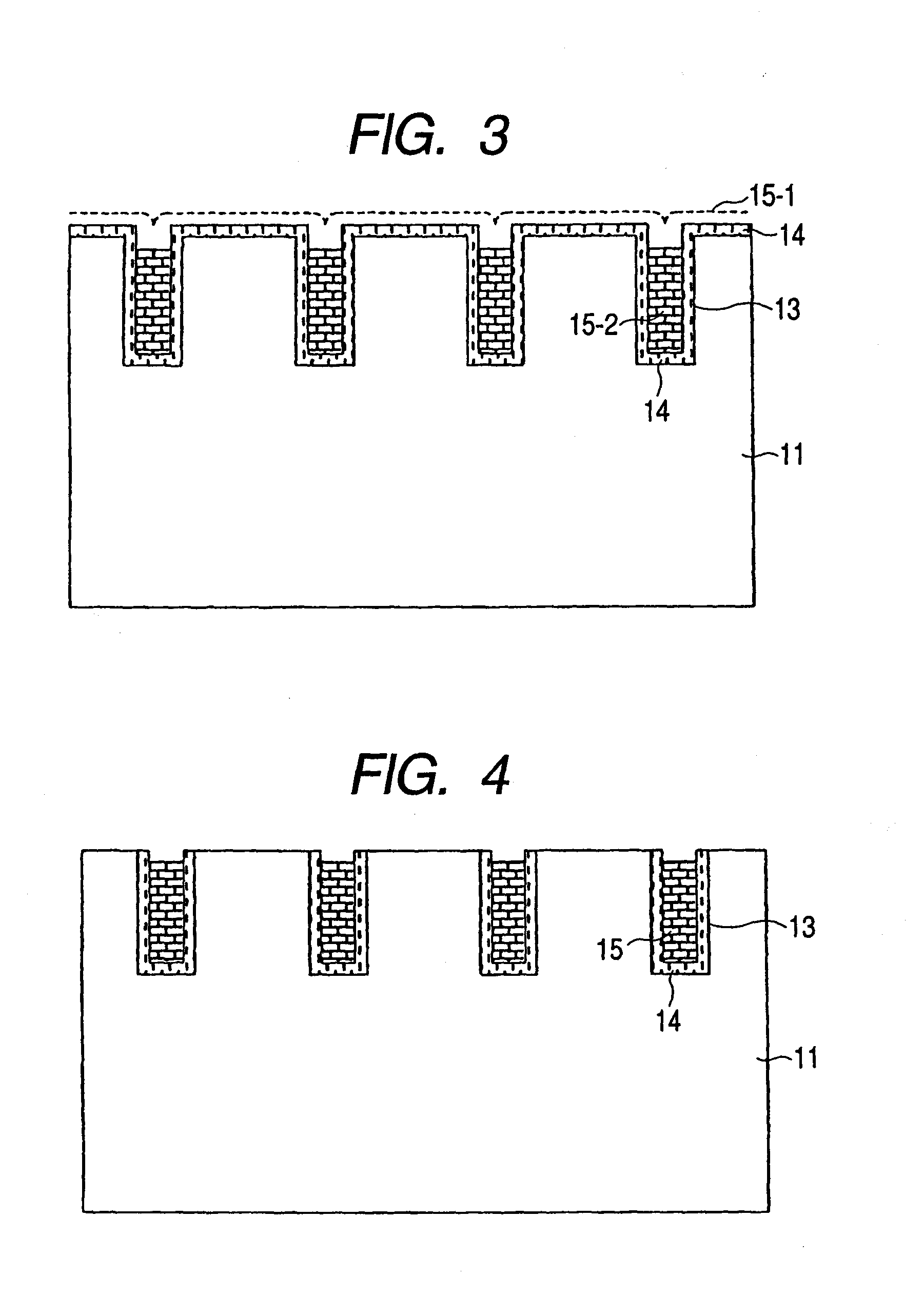
[0151]As in a related device, n−-type silicon substrate 11 is prepared as shown in FIG. 1. N−-type silicon substrate 11 has an n−-region that becomes a base region on the surface thereof whose direction of crystal plane is (100) and has a resistivity of 30 Ωcm. On the surface of n−-type silicon substrate 11, a resist pattern is formed for forming a guard ring (a kind of a voltage blocking structure with a function of reducing electric field strength on a surface—not shown), p-type impurity ions are implanted, and heat treatment is carried out after the resist is removed. T...

example 2

[0163]Example 2 of the vertical and trench type insulated gate MOS semiconductor device according to the invention will be explained with reference to FIG. 15. In Example 2, a vertical IGBT with a breakdown voltage of 600 V is taken as an example of a power vertical and trench type insulated gate MOS semiconductor device and its structure will be shown.

[0164]The process of manufacturing the IGBT is the same as that in Example 1 with only the shapes, arrangements and dimensions of p+-type body region 27, n+-type emitter region 26 and contact region 41 of a metal / semiconductor layer being modified from those in Example 1. The main modification is that the angle formed by trench 13 and a side of n+-type emitter region 26 intersecting trench 13 is 45 degrees rather than 90 degrees and that the length of contact region 41 of the metal / semiconductor layer in the longitudinal direction of trench 13 is longer than the length of n+-type emitter region 26 in the longitudinal direction of tren...

example 3

[0167]Example 3 of the vertical and trench type insulated gate MOS semiconductor device according to the invention will be explained with reference to FIG. 16. In Example 3, a vertical IGBT with a breakdown voltage of 600 V is taken as an example of a power vertical and trench type insulated gate MOS semiconductor device and its structure will be shown.

[0168]The process of manufacturing the IGBT is the same as that in Example 1 with only the shapes, arrangements and dimensions of p+-type body region 37, n+-type emitter region 36 and contact region 42 of a metal / semiconductor layer being modified from those in Example 1. The main modification is that the angle formed by trench 13 and a side of n+-type emitter region 36 intersecting trench 13 is 45 degrees rather than 90 degrees and that contact region 42 of the metal / semiconductor layer is not provided for all of the portions in the longitudinal direction of trench 13 of n+-type emitter region 36. With contact region 42 of the metal / ...


PUM


Abstract

A vertical and trench type insulated gate MOS semiconductor device is provided in which the surfaces of p-type channel regions and the surfaces of portions of an n-type semiconductor substrate alternate in the longitudinal direction of the trench between the trenches arranged in parallel, and an n+-type emitter region selectively formed on the surface of the p-type channel region is wide by the side of the trench and becomes narrow toward the center point between the trenches. This enables the device to achieve low on-resistance and enhanced turn-off capability.

Description

CROSS REFERENCE TO RELATED APPLICATIONS[0001]This application claims priority from application Serial No. JP 2006-122811, filed on Apr. 27, 2006; JP 2006-187439 filed on Jul. 7, 2006; and JP 2007-058029, filed on Mar. 8, 2007, the contents of each these being incorporated herein in their entirety.BACKGROUND OF THE INVENTION[0002]A. Field of the Invention[0003]The present invention relates to a power MOS semiconductor device having a trench type insulated gate. Further in detail, the invention relates to a vertical power MOS semiconductor device having a trench type insulated gate structure with a trench, a gate insulator film and a control electrode, the trench being formed in a semiconductor substrate in a stripe-like surface pattern, the gate insulator film being formed on the sidewall surface of the trench and the control electrode being buried in the trench with the gate insulator film interposed between. In the structure, first conductivity type regions and second conductivity ...

Claims


Application Information

Patent Timeline
Patent Type & Authority Patents(United States)
IPC IPC(8): H01L29/76
CPCH01L29/0696H01L29/7397H01L29/66348
Inventor YOSHIKAWA, KOHWAKIMOTO, HIROKIOTSUKI, MASAHITO
Owner FUJI ELECTRIC CO LTD
Why Eureka
Try Eureka