Method for measuring a pattern dimension using a scanning electron microscope

a scanning electron microscope and pattern technology, applied in the direction of material analysis using wave/particle radiation, instruments, analogue processes for specific applications, etc., can solve the problem of large processing time for apparatus parameter estimation, measurement error dependent on the shape of target pattern, and electron beam simulation for library creation does not produce correct results, etc. problem, to achieve the effect of reducing the number of parameters, reducing the time required for estimation, and increasing the number of parameters

Active Publication Date: 2010-06-08
HITACHI HIGH-TECH CORP
View PDF12 Cites 14 Cited by
  • Summary
  • Abstract
  • Description
  • Claims
  • Application Information

AI Technical Summary

Benefits of technology

[0009]In accordance with predicted values of shapes and dimensional changes of a measurement target sample, the present invention performs an electron beam simulation to create SEM images for cases where these shape changes are generated, and records (stores) simulation images of various shapes as a library. Here, the term “simulation” indicates to a general method for simulating a physical phenomenon on the basis of a model. In the present invention, an electron beam simulation for library creation especially indicates simulating a process of electron microscope image creation in an SEM and calculating the relationship between a measurement target shape and electron microscope image waveform. The electron beam simulation for library creation does not produce correct results if an inappropriate model is used. When the electron beam simulation for library creation is to be conducted, the present invention enhances the accuracy of electron beam simulation and measurements based on electron beam simulation by providing means for properly setting up the characteristics of an apparatus that acquires an electron microscope image. In this instance, various apparatus characteristic parameters (electron optics resolution, beam divergence half angle, aberration coefficients, etc.) used for the electron beam simulation are the design information about electron optics, the values calculated in accordance with the design information, or the values obtained in advance by measuring actual apparatus characteristic with measurement means. When measurements are to be made, an SEM image of a measurement target pattern is picked up and compared with various SEM waveforms recorded (stored) in a prepared library (a first simulated waveform or a second simulated waveform, which is created when the first simulated waveform is subjected to interpolation, Gaussian filtering, or the like), to select the most similar SEM waveform. This makes it possible to make high-precision measurements while considering a three-dimensional shape.
[0019]As described above, the present invention can reduce the number of parameters to be estimated because it predetermines some or all of the apparatus parameters of the electron microscope in accordance with design values or measured values, instead of estimating by nonlinear least-square method. When the nonlinear least-squares method is used, the time required for estimation increases with an increase in the number of parameters to be estimated. If similar signal waveforms are given with a certain number of parameter combinations, the results might not converge. If a large number of parameters are involved, the estimation accuracy for each parameter may decrease due to noise, thereby degrading measurement repeatability.
[0020]In other words, the present invention can avoid vagueness in parameter estimation because it predetermines the apparatus parameters of the electron microscope by another method. Therefore, the present invention makes it possible to make stable, high-speed CD-SEM measurements.
[0021]The present invention can decrease the number of parameters to be estimated during the use of a model-based measurement method. Therefore, the present invention makes it possible to achieve consistent estimation and reduce the calculation time required for measurement.
[0022]Further, the present invention provides enhanced electron beam simulation accuracy by reflecting the apparatus characteristics of the CD-SEM in electron beam simulation. As a result, the accuracy of the model-based measurement method is also improved.
[0023]Furthermore, the present invention determines the apparatus characteristics of the CD-SEM in accordance with electron optics design values or predetermines the apparatus characteristic by allowing measurement means to make measurements, and reflects the determined apparatus characteristic in electron beam simulation. Therefore, the present invention also makes it possible to reduce measurement variations among a plurality of or CD-SEMs.

Problems solved by technology

As described in conjunction with the above background art, a measurement error dependent on the shape of a target pattern occurs when the dimensions of a semiconductor pattern are measured with a CD-SEM.
Further, apparatus parameter estimation takes a large amount of processing time.
The electron beam simulation for library creation does not produce correct results if an inappropriate model is used.

Method used


Image

  • Method for measuring a pattern dimension using a scanning electron microscope
  • Method for measuring a pattern dimension using a scanning electron microscope
  • Method for measuring a pattern dimension using a scanning electron microscope

Examples


first embodiment

(Providing Increased Accuracy by Reflecting Apparatus Characteristics: Library Creation Procedure)

[0043]A first embodiment of the method and apparatus (system) for measuring a measurement target pattern according to the present invention will now be described by explaining about a basic procedure and system configuration for the use of a CD-SEM with reference to FIGS. 1 to 6.

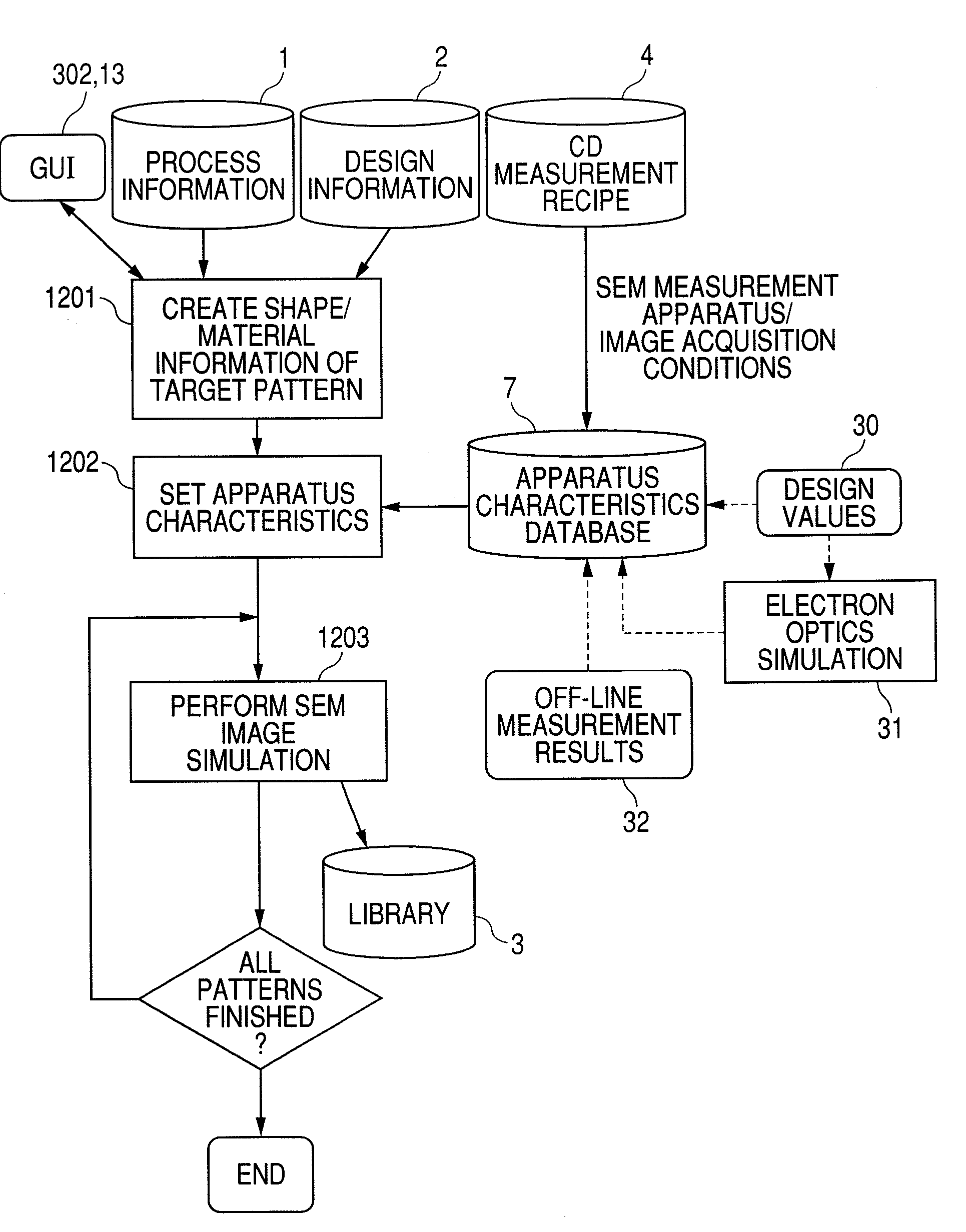
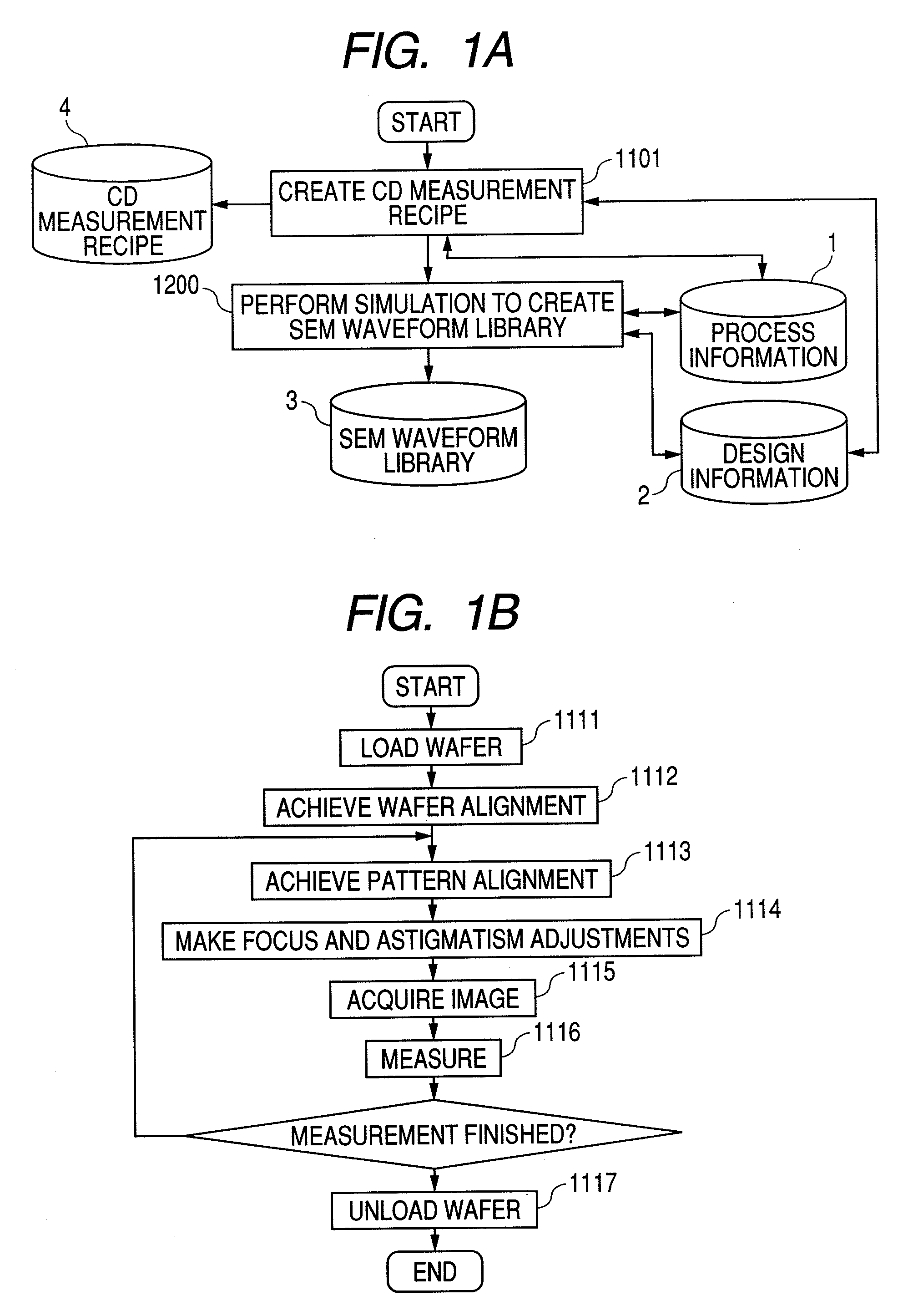
[0044]FIG. 1A shows an embodiment of a procedure for creating a CD measurement recipe 4 and SEM waveform library 3 for image acquisition, which are used by the method and apparatus (system) for measuring a pattern according to the present invention. FIG. 1B shows an embodiment of a procedure for making actual measurements.

[0045]A processing / control section 300 of a CD-SEM 10, which is shown in FIG. 4, or a CD measurement recipe creation section (not shown), which is installed in a different computer connected via an interface (network) 20, first creates a CE measurement recipe as shown in FIG. 1A (step 1101) by ...

second embodiment

(Reflecting the Information Obtained at a Design Phase-1: Registering Characteristics on an Individual Condition Set Basis)

(Reflecting the Information Obtained at a Design Phase-2: Registering Characteristics on an Individual Electron Optics Simulation / Condition Set Basis)

[0078]A second embodiment will now be described with reference to a specific procedure for reflecting the apparatus characteristics in an SEM image simulation. The second embodiment relates to the details of step 1200, which is shown in FIG. 1A. As described in conjunction with the first embodiment, the apparatus characteristics of the CD-SEM can be set from the design values if the information about incorporated performance characteristics is available. For example, the electron beam shape and aberration coefficients can be calculated by performing an electromagnetic field analysis in accordance with the design information about the electron optics. The electromagnetic field analysis is made to calculate the elect...

third embodiment

(Reflecting the Actual Apparatus Status-1: Resolution Measurement)

[0088]A third embodiment of the procedure for creating the apparatus characteristics database 7 in step 1202, which is shown in FIG. 8, will now be described. As the third embodiment, the procedure for evaluating the CD-SEM resolution with an actual image and reflecting the evaluation result in the library or matching will be described with reference to FIGS. 10A and 10B. It is difficult to obtain exactly the same performance from apparatuses manufactured in the same manner because, in reality, the employed parts vary from one unit to another and the accuracy in assembly and adjustment is limited. Even when the same CD-SEM model is manufactured, the resolution slightly varies from one unit to another. As a result, when the same sample is measured, the measured values vary from one unit to another. The third embodiment of the present invention measures the characteristics of each tool in advance, reflects the measureme...


PUM

PropertyMeasurementUnit
sidewall anglesaaaaaaaaaa

Abstract

To provide a consistent, high-speed, high-precision measurement method based on an electron beam simulation by reflecting the apparatus characteristics of a CD-SEM in an electron beam simulation, the present invention discloses a method for measuring a measurement target pattern with a CD-SEM, the method comprising the steps of performing an electron beam simulation on various target pattern shapes, which is reflected apparatus characteristic and image acquisition conditions; creating SEM simulated waveforms; storing a combination of the created SEM simulated waveforms and pattern shape information corresponding to the created SEM simulated waveforms as a library; comparing an acquired actual electron microscope image with the SEM simulated waveforms; selecting the SEM simulated waveform that is most similar to the actual electron microscope image; and estimating the shape of the measurement target pattern from the pattern shape information corresponding to the selected SEM simulated waveform.

Description

BACKGROUND OF THE INVENTION[0001]The present invention relates to a method and system for evaluating the shape of a circuit pattern, which is formed on a wafer during a semiconductor manufacturing process, by using an electron microscope image of the circuit pattern, which is obtained by an electron microscope, and more particularly to a method for measuring a measurement target pattern with an electron microscope.[0002]In a semiconductor wafer manufacturing process, a multilayer pattern formed on a wafer has been rapidly rendered microscopic. Therefore, process monitoring for checking whether the pattern is formed on the wafer in compliance with design specifications has become increasingly important. The wiring widths of transistor gate wiring patterns and other similar wiring patterns are significantly associated with device performance. Therefore, it is particularly important that a wiring manufacturing process for such wiring patterns be properly monitored.[0003]A critical dime...

Claims


Application Information

Patent Timeline
Patent Type & Authority Patents(United States)
IPC IPC(8): G06F7/60G01N23/00G06G7/48G21K7/00G06G7/62G06F17/10G06F17/50
CPCG01N23/2251H01J2237/24578G01N2223/6116
Inventor TANAKA, MAKISHISHIDO, CHIE
Owner HITACHI HIGH-TECH CORP
Why Eureka
Try Eureka