
CMOS image sensor and method for fabricating the same

a technology of image sensor and manufacturing method, which is applied in the direction of solid-state devices, semiconductor devices, radio frequency controlled devices, etc., can solve the problems of difficult to reduce the size of ccds, complex fabrication process of ccds, and high power consumption, so as to facilitate the control of a doping profile and improve the dark current and light sensitivity characteristics of a photodiode.

Inactive Publication Date: 2010-05-11
DONGBU HITEK CO LTD
View PDF6 Cites 1 Cited by
  • Summary
  • Abstract
  • Description
  • Claims
  • Application Information

AI Technical Summary

Benefits of technology

The patent text describes a method for fabricating a complementary metal oxide semiconductor (CMOS) image sensor (CIS) that improves the dark current and light sensitivity characteristics of a photodiode. The method includes implanting first conductive type dopants in a semiconductor substrate to form a photodiode region, implanting second conductive type dopants in the photodiode region to form a second conductive type diffusion region, and implanting fluorine ions in the second conductive type diffusion region to form a fluorine diffusion region. The CIS includes an epitaxial layer formed in a semiconductor substrate, a photodiode region formed in the epitaxial layer, a first diffusion region formed in the photodiode region, and a second diffusion region formed in the first diffusion region. The technical effect of this method is to enhance the performance of CIS by improving the dark current and light sensitivity characteristics of the photodiode.

Problems solved by technology

CCDs are complex and have high power consumption.
In addition, the fabrication process of CCDs is complex because the process requires a multi-step photo process.
It is also difficult to decrease the size of CCDs because of the difficulty in integrating a controller, a signal processor, and an analog-to-digital (A / D) converter in a chip of the CCD.
This may cause a movement of the electrons to the photodiode region to thereby generate an undesired signal in the surface.
However, a portion of the electrons remains without removing or coupling with holes and thus, causes a dark current thereby deteriorating a product characteristic of the CMOS sensor.
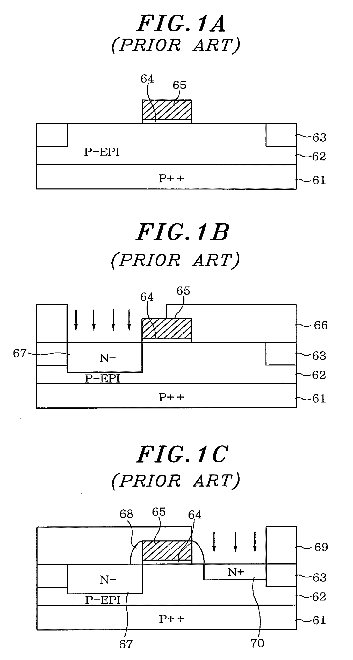
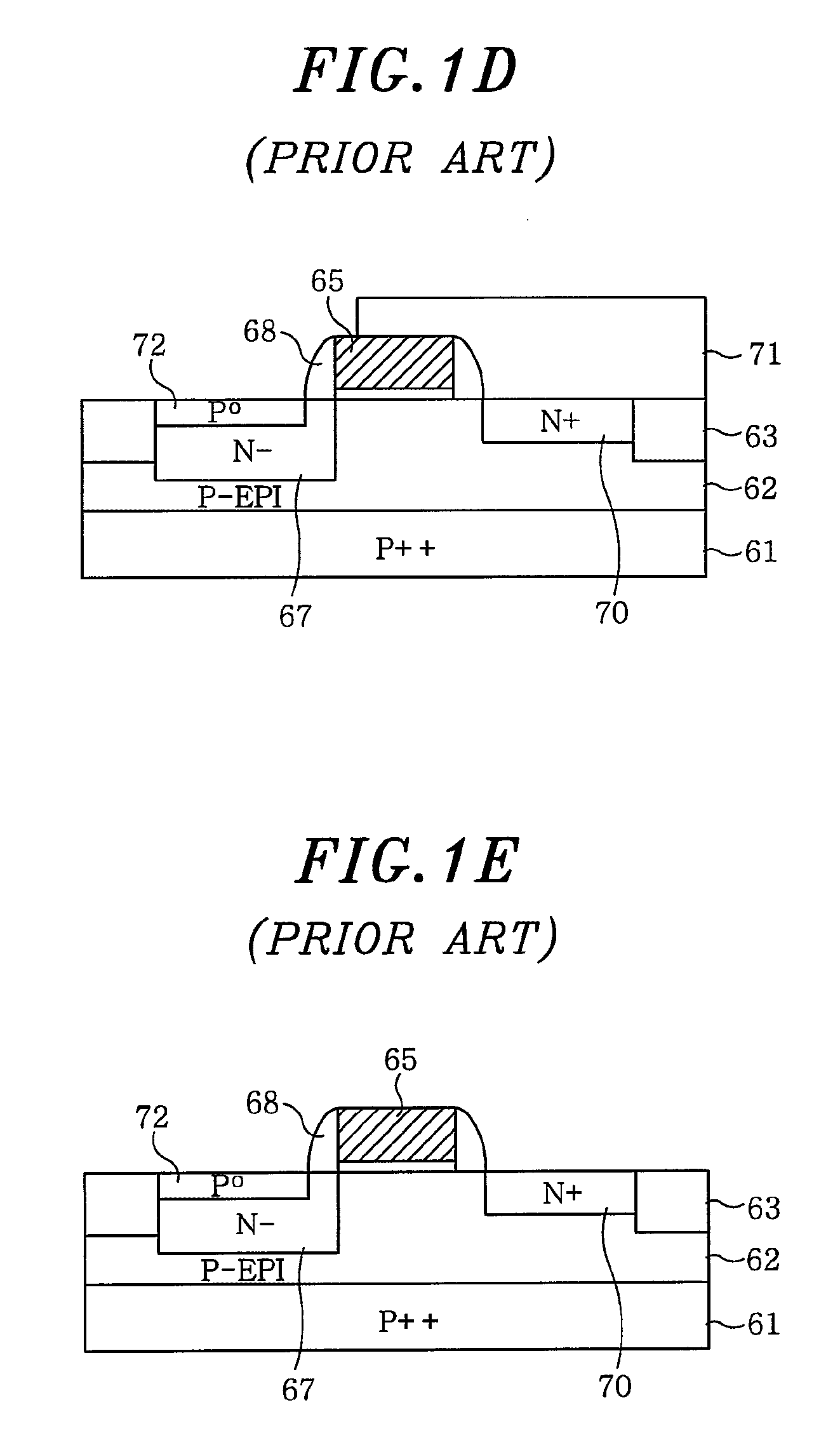
However, in the prior art, there is a limitation in controlling the diffusion of boron (B) having a small mass and fast diffusion.
Accordingly, low energy ion implantation makes it difficult to realize a concentration profile in a desired form.
This leads to the generation of an unnecessary signal to thereby produce a noise in images.
Also, it is difficult to control the diffusion of P type dopants into the N type region and therefore, a light sensitivity characteristic, in particular, sensitivity to a blue color-based short wavelength light is deteriorated.
Accordingly, in the case of low energy, as disclosed in FIG. 3B, it is difficult to control a doping profile (a concentration profile) when a thermal process is performed after ion implantation of boron.

Method used


Image

  • CMOS image sensor and method for fabricating the same
  • CMOS image sensor and method for fabricating the same
  • CMOS image sensor and method for fabricating the same

Examples


Embodiment Construction

[0019]In general, example embodiments of the invention relate to a complementary metal oxide semiconductor (CMOS) image sensor (CIS) and a method for fabricating the same. In one example embodiment, the example method for fabricating the CIS facilitates control of a doping profile and improves dark current and light sensitivity characteristics of a photodiode.

[0020]In one example embodiment, a method for fabricating a CIS includes implanting first conductive type dopants in a semiconductor substrate to form a photodiode region in a surface of the semiconductor substrate, implanting second conductive type dopants in the photo diode region to form a second conductive type diffusion region, and implanting fluorine ions in the second conductive type diffusion region to form a fluorine diffusion region.

[0021]In another example embodiment, a CIS includes an epitaxial layer formed in a semiconductor substrate, a photodiode region formed in the epitaxial layer, a first diffusion region form...


PUM


Abstract

A complementary metal oxide semiconductor (CMOS) image sensor (CIS) and a method for fabricating the same. A method for fabricating a CIS includes implanting first conductive type dopants in a semiconductor substrate to form a photodiode region in a surface of the semiconductor substrate, implanting second conductive type dopants in the photo diode region to form a second conductive type diffusion region, and implanting fluorine ions in the second conductive type diffusion region to form a fluorine diffusion region.

Description

CROSS-REFERENCE TO RELATED APPLICATION[0001]This application claims priority to Korean Application No. 10-2006-0135685, filed on Dec. 27, 2006, which is incorporated herein by reference in its entirety.BACKGROUND[0002]1. Field of the Invention[0003]The present invention relates to a CMOS image sensor and a method for fabricating the same.[0004]2. Description of the Related Art[0005]Generally, an image sensor is a semiconductor device used to convert an optical image into an electrical signal. Image sensors may generally be classified as either charge-coupled devices (CCDs) or complementary metal oxide semiconductor (CMOS) image sensors (CISs).[0006]A CCD has a plurality of photodiodes (PDs) arranged in matrix form for converting an optical signal into an electrical signal. A CCD includes a plurality of vertical charge coupled devices (VCCDs), a horizontal charge coupled device (HCCD), and a sense amplifier. The VCCDs are formed between respective PDs arranged in matrix form and tran...

Claims


Application Information

Patent Timeline
Patent Type & Authority Patents(United States)
IPC IPC(8): H01L21/8238H01L21/00H01L29/04H01L31/062H01L31/036H01L21/04H01L21/329
CPCH01L27/14603H01L31/0288H01L27/14689Y02E10/50Y10S438/923H01L27/146
Inventor LEE, JOUNG HO
Owner DONGBU HITEK CO LTD
Learn More