
Shielding film, shielded printed circuit board, shielded flexible printed circuit board, method of manufacturing shielding film, and method of manufacturing shielded printed circuit board

a technology of printed circuit board and shielding film, which is applied in the direction of paper/cardboard containers, transportation and packaging, synthetic resin layered products, etc., can solve the problems of blockage resistance deterioration, metal layer breakage such as cracking, fracture or the like, and does not serve as a protective layer, etc., to achieve excellent flexibility and excellent assembly efficiency

Active Publication Date: 2010-05-04
NIPPON MEKTRON LTD +1
View PDF17 Cites 19 Cited by
  • Summary
  • Abstract
  • Description
  • Claims
  • Application Information

AI Technical Summary

Benefits of technology

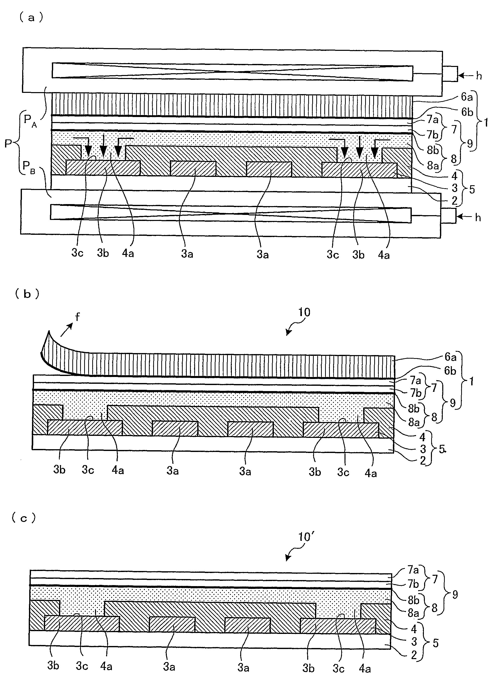
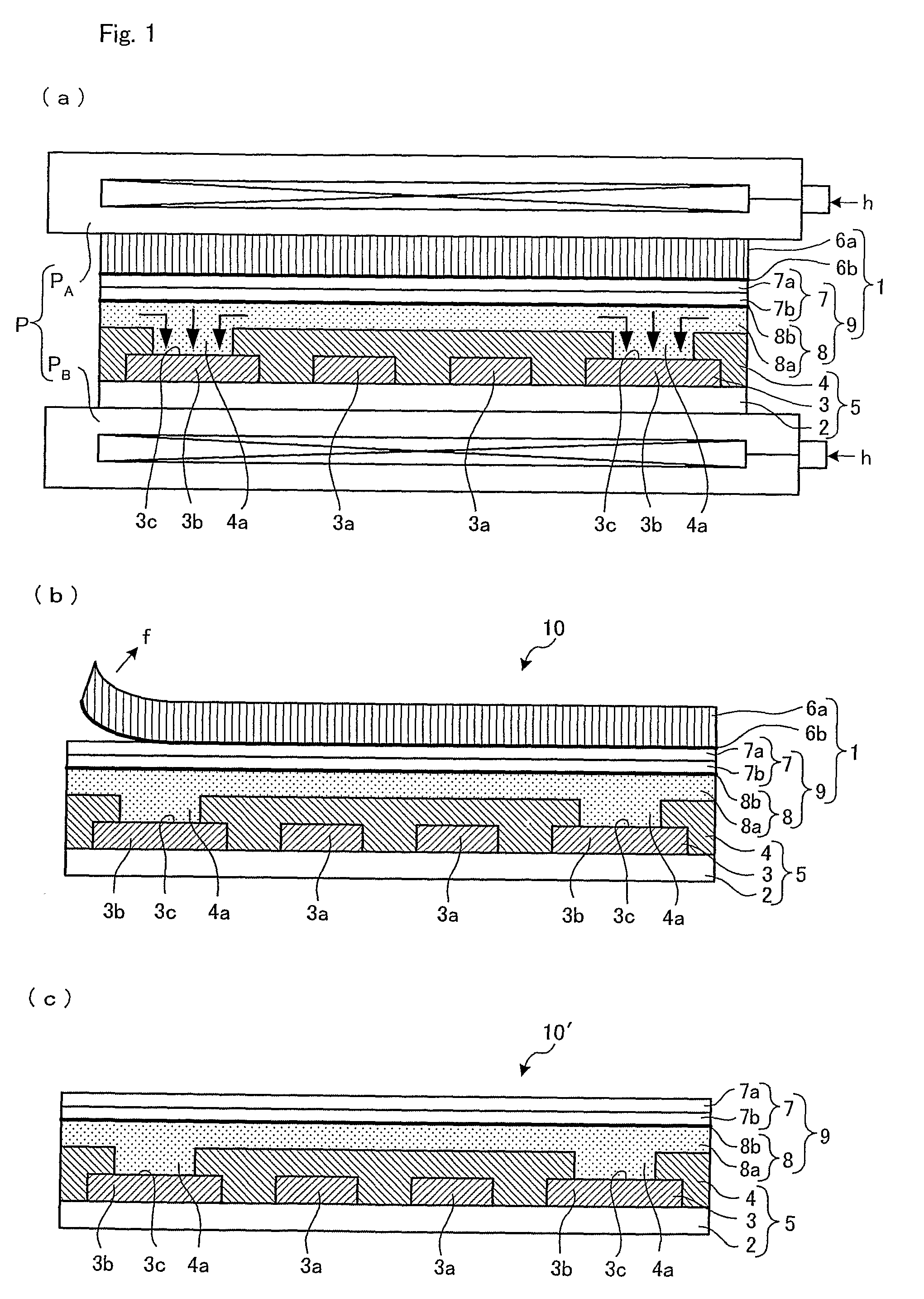
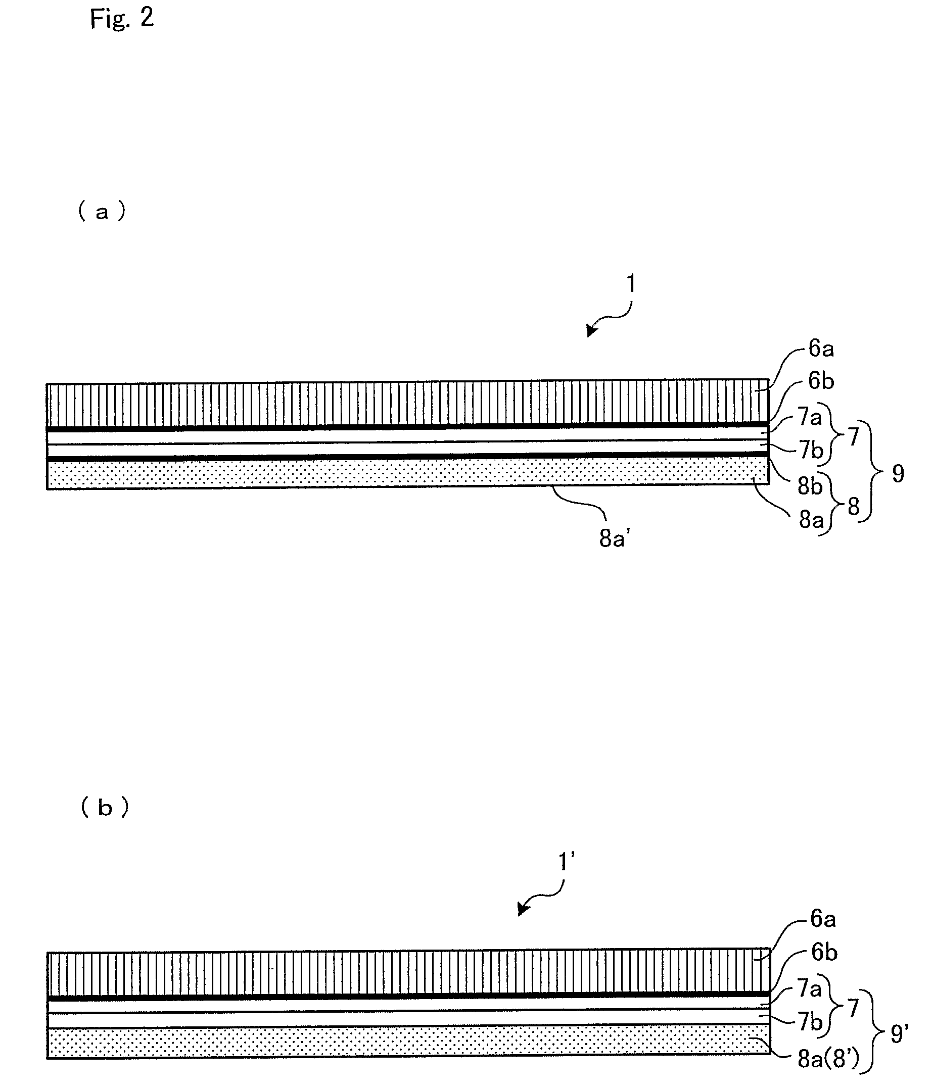
The invention provides a shielding film, a shielded printed circuit board, and a shielded flexible printed circuit board that have a cover film with high hardness and excellent abrasion resistance, as well as blocking resistance. The cover film is made of a hard layer and a soft layer, and the soft layer is cushioning the impact of the hard layer. The shielding film has excellent flexibility and can be thin and flexible. The shielded printed circuit board has a metal layer and a foundation including printed circuits via an adhesive layer, and the cover film is adhered to the metal layer. The adhesive layer may be a conductive adhesive that can electrically connect the metal layer to the grounding circuit. The invention also provides a method for manufacturing the shielding film and the shielded printed circuit board.

Problems solved by technology

However, the following problems are generated.
For example, a shielded FPC used for a moving unit such as a mobile phone, a printer, or the like, is worn by rubbing against another part such as a housing or the like, and does not serve as a protective layer after the release of the separation film.
As a result, breakage such as a cracking, fracture, or the like occurs in the metal layer.
As a result, the blocking resistance deteriorates.
However, the cover film having high hardness is brittle.
For this reason, when the shielding film using the cover film is adhered on a foundation film including printed circuits, the cover film having high hardness cracks due to the concavity and convexity of the insulation removed portions of the insulating film.

Method used


Image

  • Shielding film, shielded printed circuit board, shielded flexible printed circuit board, method of manufacturing shielding film, and method of manufacturing shielded printed circuit board
  • Shielding film, shielded printed circuit board, shielded flexible printed circuit board, method of manufacturing shielding film, and method of manufacturing shielded printed circuit board
  • Shielding film, shielded printed circuit board, shielded flexible printed circuit board, method of manufacturing shielding film, and method of manufacturing shielded printed circuit board

Examples


examples

[0071]Next, the results of the evaluation tests, which are performed with the examples of the invention, and comparative examples will be described.

[0072](1) Rubbing Test

[0073]Specimens: Each of the shielding films, which have cover films 7 according to first to third examples and first to third comparative examples shown in Table 1, is adhered to a CCL 20 as shown in FIG. 7(a), and the shielding film and the CCL are then heated and pressed to prepare each sheet having a width of 50 mm and a length of 140 mm. The sheets have been used as the specimens. Here, the CCL 20 is obtained by adhering a polyimide film 23 to a copper foil 21 by an adhesive 22. The thickness of each layer is as follows: the thickness of the hard layer 7a is 2 μm, the thickness of the soft layer 7b is 3 μm, the thickness of the metal layer 8b is 0.15 μm, the thickness of the adhesive layer 8a having conductivity is 20 μm, the thickness of the copper foil 21 is 18 μm, the thickness of the adhesive 22 is 17 μm, a...

first example

[0087]The following shielding film is used as a first example. The shielding film includes a hard layer, a soft layer, and a shielding layer. The hard layer has a thickness of 2 μm and is formed by mixing 100 parts by weight of ultraviolet curing polyfunctional acrylate and 50 parts by weight of ultraviolet curing bifunctional acrylate to each other. The soft layer has a thickness of 3 μm, and is made of a modified epoxy resin. Furthermore, the shielding layer is formed on the soft layer. Then, abrasion resistance, blocking resistance, and embedding resistance has been evaluated for the first example. In this case, the thickness of an evaporated silver layer, which is the metal layer 8b of the shielding layer 8, has been set to 0.15 μm, the thickness of the adhesive layer 8a having conductivity has been set to 20 μm, the thickness of the insulating layer has been set to 40 μm, and the diameter of the insulation removed portion has been set to 1.4 mmφ (hereinafter, the structures of ...

second example

[0088]The following shielding film is used as a second example. The shielding film includes a hard layer, a soft layer, and a shielding layer. The hard layer has a thickness of 2 μm and is formed by mixing 100 parts by weight of ultraviolet curing polyfunctional acrylate and 150 parts by weight of ultraviolet curing bifunctional acrylate to each other. The soft layer has a thickness of 3 μm, and is made of a modified epoxy resin. Furthermore, the shielding layer is formed on the soft layer. Then, abrasion resistance, blocking resistance, and embedding resistance has been evaluated for the second example. The results thereof are shown in Table 1. In addition, a flexible duration has been evaluated through the sliding resistance test. The result thereof is shown in FIG. 9.


PUM

PropertyMeasurementUnit
thicknessaaaaaaaaaa
thicknessaaaaaaaaaa
distanceaaaaaaaaaa

Abstract

The invention includes a shielding film, which does not have breakage of a metal layer, and has excellent abrasion resistance and blocking resistance, and does not crack. The cover film 7 is provided on one surface of a separation film 6a, and an adhesive layer 8a is formed on the surface of the cover film 7 opposite to the separation film 6a via the metal layer. The cover film 7 has at least one hard layer 7a and at least one soft layer 7b, and the surface of the cover film 7 facing the separation film 6a is composed of the hard layer 7a.

Description

TECHNICAL FIELD[0001]The present invention relates to a shielding film shielding a printed circuit board etc. which is used in a device such as a computer, a communication device, a printer, a mobile phone, a video camera, or the like, a method of manufacturing the shielding film, a shielded printed circuit board and a shielded flexible printed circuit board that are manufactured by using the shielding film, and a method of manufacturing a shielded printed circuit board.BACKGROUND ART[0002]A flexible printed circuit board (hereinafter, referred to as ‘FPC’) has a printed circuit, which is provided on at least one surface of a flexible insulating film such as a polyimide film or a polyester film with or without an adhesive between the printed circuit and the flexible film. According to need, a flexible insulating film having openings is adhered on the surface of the printed circuit by an adhesive, or a protective layer is formed on the surface of the printed circuit. The openings are...

Claims


Application Information

Patent Timeline
Patent Type & Authority Patents(United States)
IPC IPC(8): H05K9/00
CPCH05K1/0218H05K3/281H05K1/0393H05K3/321Y10T428/24983H05K2201/0195H05K2203/066Y10T156/10H05K3/4652H05K1/02H05K9/00
Inventor HASHIMOTO, KAZUHIROMORIMOTO, SYOHEIKAWAKAMI, YOSHINORIKAMINO, KENJIEBIHARA, SATOSHITANAKA, HIDEAKIAKATSUKA, TAKAHISA
Owner NIPPON MEKTRON LTD
Learn More