Solid-state image pickup device, drive method therefor and camera

a solid-state image and pickup device technology, applied in the direction of solid-state device signal generators, picture signal generators, television systems, etc., can solve the problems of sacrificing sensitivity, affecting the resolution, and long transfer processing time, so as to achieve the effect of reducing resolution and sacrificing sensitivity

Inactive Publication Date: 2010-04-20
PANASONIC SEMICON SOLUTIONS CO LTD
View PDF21 Cites 2 Cited by
  • Summary
  • Abstract
  • Description
  • Claims
  • Application Information

AI Technical Summary

Benefits of technology

The present invention provides a solid-state image pickup device that can read imaging signals quickly without sacrificing sensitivity or resolution. The device includes a plurality of optoelectronic transducers arranged in an array, vertical transfer sections for reading charges from the transducers, a horizontal transfer section for horizontally transferring the charges, and a control section for outputting the necessary signals to perform the vertical and horizontal transfer operations. The device can use either a complementary color filter or a primary color filter, and can read from either a single column or a combination of columns. The control section can also output the necessary signals to perform the horizontal transfer in a different direction every field, allowing for more efficient use of the transducers. Overall, the device allows for high-speed readout of imaging signals with no sacrifice in sensitivity or resolution.

Problems solved by technology

However, a solid-state image pickup device having a large number of pixels requires a comparatively long time to read all signals from pixels, and therefore cannot output signals at a frame rate of normal TV signals necessary for the monitor.
However, in the conventional solid-state image pickup device in which signal charges from one row are transferred vertically in one horizontal scanning period, the transfer processing time is long when the number of pixels is large.
Even if charges from two pixels are mixed together in the vertical transfer section, it takes long time to output signal charges corresponding to the entire screen, and thus it is impossible to output a sufficient number of frames per unit time.
Even if the scanning mode is converted using a memory and the like, display of moving images smooth in motion in real time is unattainable.
In the case that pixels are simply thinned so that 2R-G and 2B-G lines are output line-sequentially by a general drive method for a solid-state image pickup device for realizing the monitor mode described above, equal sampling intervals are not obtainable due to the pattern of a general color filter formed on the solid-state image pickup device, resulting in considerable degradation in image quality and sensitivity.
In the case of adopting a method of mixing data of the same color so that 2R-G and 2B-G lines are output line-sequentially, also, the sampling intervals are not equal between a given horizontal line and the next horizontal line, resulting in degradation in image quality.
Therefore, in a general primary color filter array, it is difficult to perform high-speed, high-sensitivity and high-quality readout.
If this drive method is adopted for an interlaced scan CCD, the gate structure of the CCD will become very complicate, and thus the number of signals required for the control will increase.
It is very inefficient to develop image processing systems separately like this to comply with the respective characteristics of the complementary color filter and the primary color filter.
This conventionally makes it difficult to shorten the time required for development of cameras and the like.

Method used


Image

  • Solid-state image pickup device, drive method therefor and camera
  • Solid-state image pickup device, drive method therefor and camera
  • Solid-state image pickup device, drive method therefor and camera

Examples


embodiment 1

[0131]In Embodiment 1, a progressive scan CCD sensor will be described as a solid-state image pickup device.

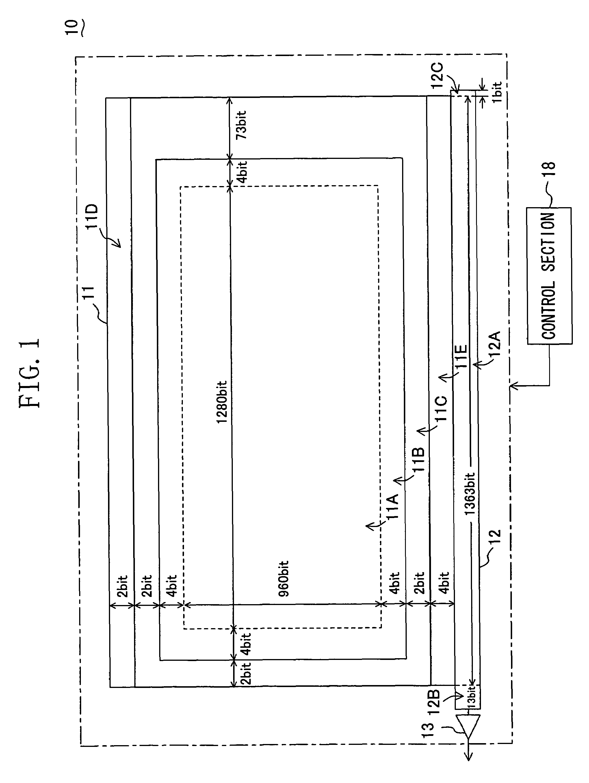
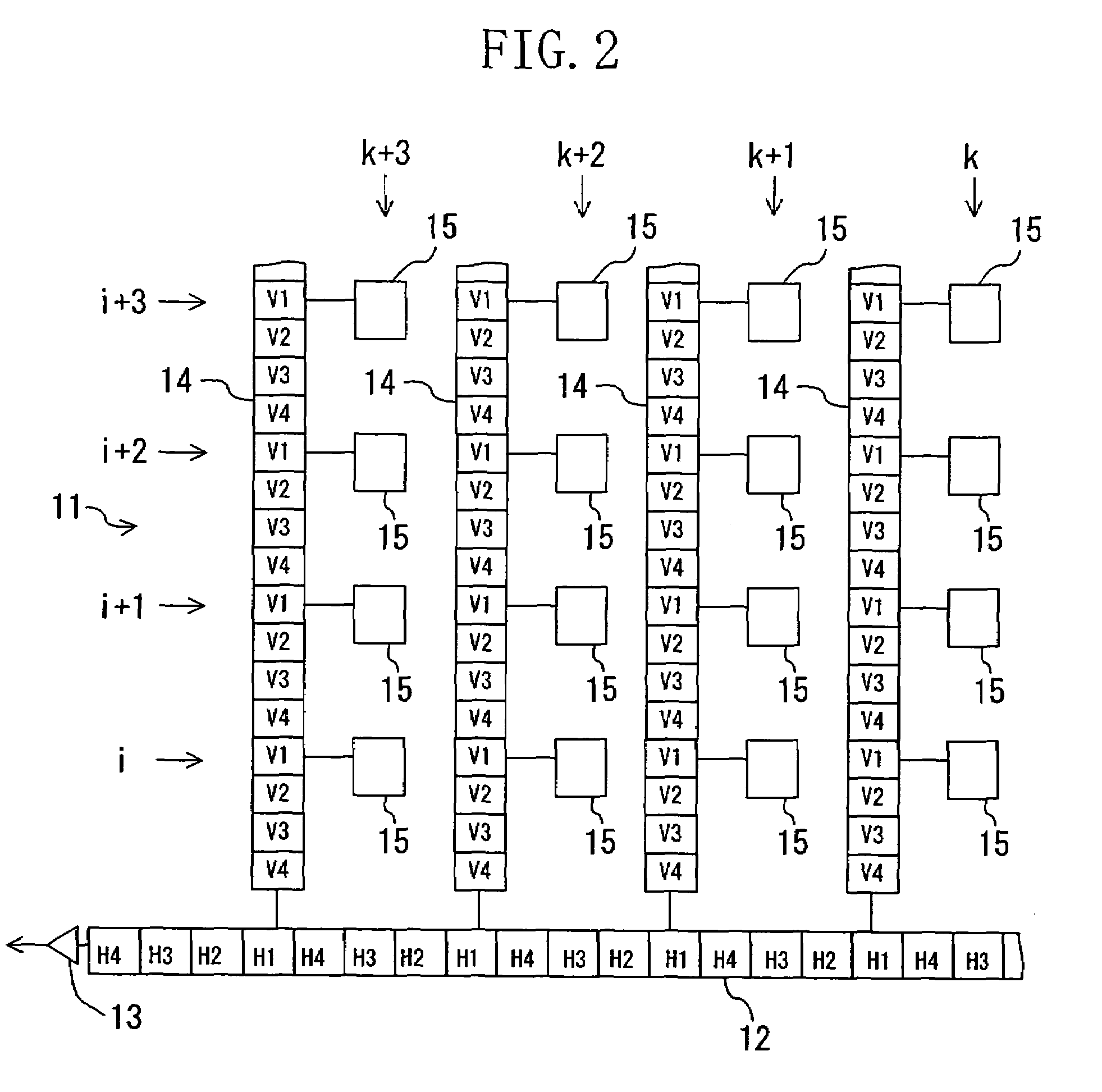
[0132]FIG. 1 is an illustration showing a configuration of a CCD sensor 10 of Embodiment 1 of the present invention. The CCD sensor 10 of FIG. 1 includes a pixel section 11, a horizontal transfer section 12, a charge detection section 13, vertical transfer sections (not shown in FIG. 1) and a control section 18. The CCD sensor 10 adopts an all pixel simultaneous independent readout scheme.

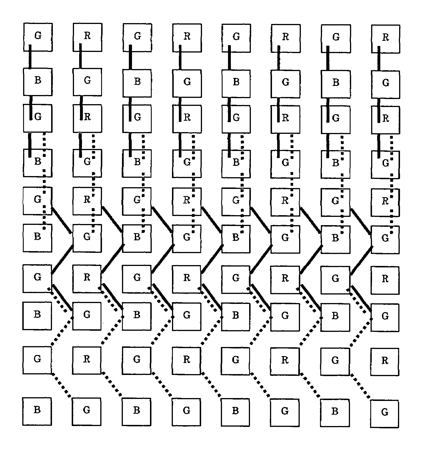
[0133]The pixel section 11 includes an effective pixel region 11A, a transient region 11B, an optical black region 11C and vertical dummy regions 11D and 11E. The effective pixel region 11A has photodiodes as optoelectronic transducers arranged in an array of 1280 (horizontal)×960 (vertical). One photodiode constitutes one pixel. Hereinafter, a horizontal line of pixels refers to a row, and a vertical line of pixels refers to a column.

[0134]The transient region 11B, which surrounds the effect...

embodiment 2

[0194]In Embodiment 2, an interlaced scan CCD sensor will be described as a solid-state image pickup device.

[0195]FIG. 17 is an illustration showing a configuration of a CCD sensor 30 of Embodiment 2 of the present invention. The CCD sensor 30 of FIG. 17 includes a pixel section 31, a horizontal transfer section 32, a charge detection section 33, vertical transfer sections (not shown in FIG. 17) and a control section 38.

[0196]The pixel section 31 includes an effective pixel region 31A, a transient region 31B, an optical black region 31C and vertical dummy regions 31D and 31E. The effective pixel region 31A has photodiodes as optoelectronic transducers arranged in an array of 1280 (horizontal)×960 (vertical). One photodiode constitutes one pixel. The regions 31A to 31E of the pixel section 31 are substantially the same in arrangement and the number of pixels as the regions 11A to 11E of the pixel section 11 of the CCD sensor 10 of FIG. 1, respectively. The transient region 31B and th...

embodiment 3

[0235]In Embodiment 3, a metal oxide semiconductor (MOS) sensor, in particular, a complementary MOS (CMOS) sensor will be described as a solid-state image pickup device.

[0236]FIG. 27 is a block diagram of a configuration of a CMOS sensor 50 of Embodiment 3 of the present invention. The CMOS sensor 50 of FIG. 27 includes a pixel address designation circuit 312, a control section 314, a sync generator 316, a timing generator 318, a vertical register (row address selection section) 322, a latch array 324, a horizontal register (column address selection section) 326, a sense amplifier 328 and a pixel section 340.

[0237]The pixel section 340 includes an effective pixel region 344, an optical black region 346 and an idle region 348. The effective pixel region 344 has photodiodes as optoelectronic transducers arranged in an array of 1280 (horizontal)×960 (vertical). One diode constitutes one pixel.

[0238]FIG. 28 is a circuit diagram showing part of the pixel section 340 in FIG. 27. Referring...


PUM


Abstract

The solid-state image pickup device of the invention includes: a plurality of optoelectronic transducers arranged in an array; a plurality of vertical transfer sections each for reading charges from optoelectronic transducers and vertically transferring the read charges; a horizontal transfer section; a charge detection section for converting the horizontally transferred charges to signal voltages and the like; and a control section. The control section outputs signals so as to obtain either a signal corresponding to the sum of charges from an optoelectronic transducer belonging to one column and belonging to one of alternately selected rows and an optoelectronic transducer belonging to a column adjacent to the one column and belonging to a row other than the alternately selected rows, or a signal corresponding to the sum of charges from optoelectronic transducers belonging to a same column, every predetermined even number of continuous rows of optoelectronic transducers.

Description

BACKGROUND OF THE INVENTION[0001]The present invention relates to a solid-state image pickup device and a camera using the same.[0002]With increase of requests for higher image quality and higher-level functions of a camera using a solid-state image pickup device such as a charge-coupled device (CCD) (note that the “camera” as used herein only refers to such a camera using a solid-state image pickup device), the number of pixels of the device is becoming larger. Many of recent-model cameras are equipped with a monitor such as a liquid crystal display for monitoring an object to be imaged.[0003]To monitor an object to be imaged reliably, the frame rate should not be so low. As the monitor, a liquid crystal TV display is often used, and in this case, signals similar to those for normal TV display must be supplied. However, a solid-state image pickup device having a large number of pixels requires a comparatively long time to read all signals from pixels, and therefore cannot output si...

Claims


Application Information

Patent Timeline
Patent Type & Authority Patents(United States)
IPC IPC(8): H04N3/14H04N5/335H04N3/15H04N9/04
CPCH04N9/045H04N3/155H04N25/42H04N25/441H04N25/46H04N25/73H04N25/76
Inventor IMAMURA, KUNIHIROFUJII, TOSHIYATASHIRO, SHINICHI
Owner PANASONIC SEMICON SOLUTIONS CO LTD
Why Eureka
Try Eureka