
Voltage controlled oscillator with switching bias

a voltage control and oscillator technology, applied in the direction of oscillator, pulse automatic control, electrical equipment, etc., can solve the problems of unstabilized operation of the voltage control oscillator, increase in the chip area, etc., to reduce the overall chip area, enhance phase noise characteristics, and reduce flicker noise of the bias circuit

Inactive Publication Date: 2010-03-09
ELECTRONICS & TELECOMM RES INST
View PDF12 Cites 10 Cited by
  • Summary
  • Abstract
  • Description
  • Claims
  • Application Information

AI Technical Summary

Benefits of technology

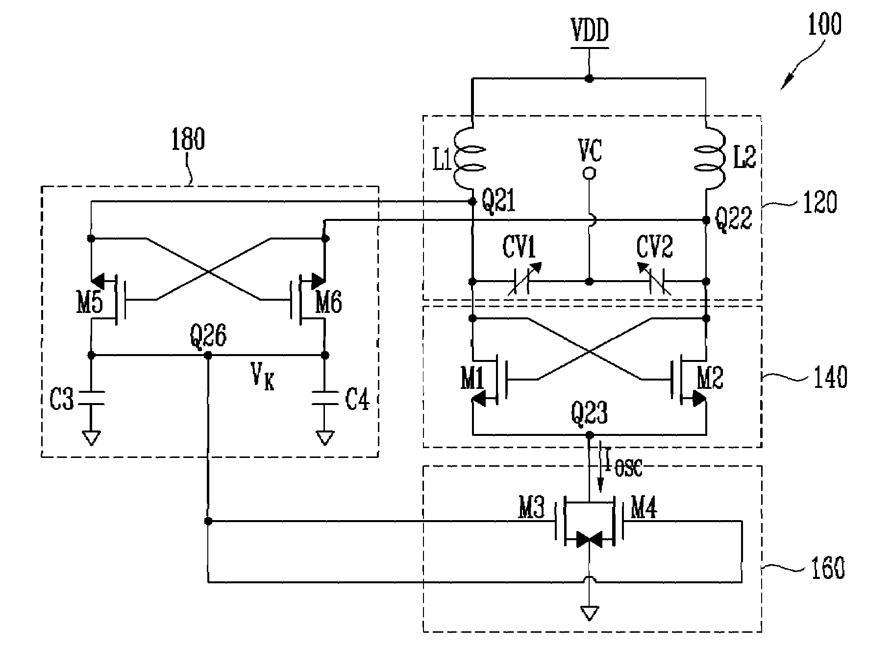
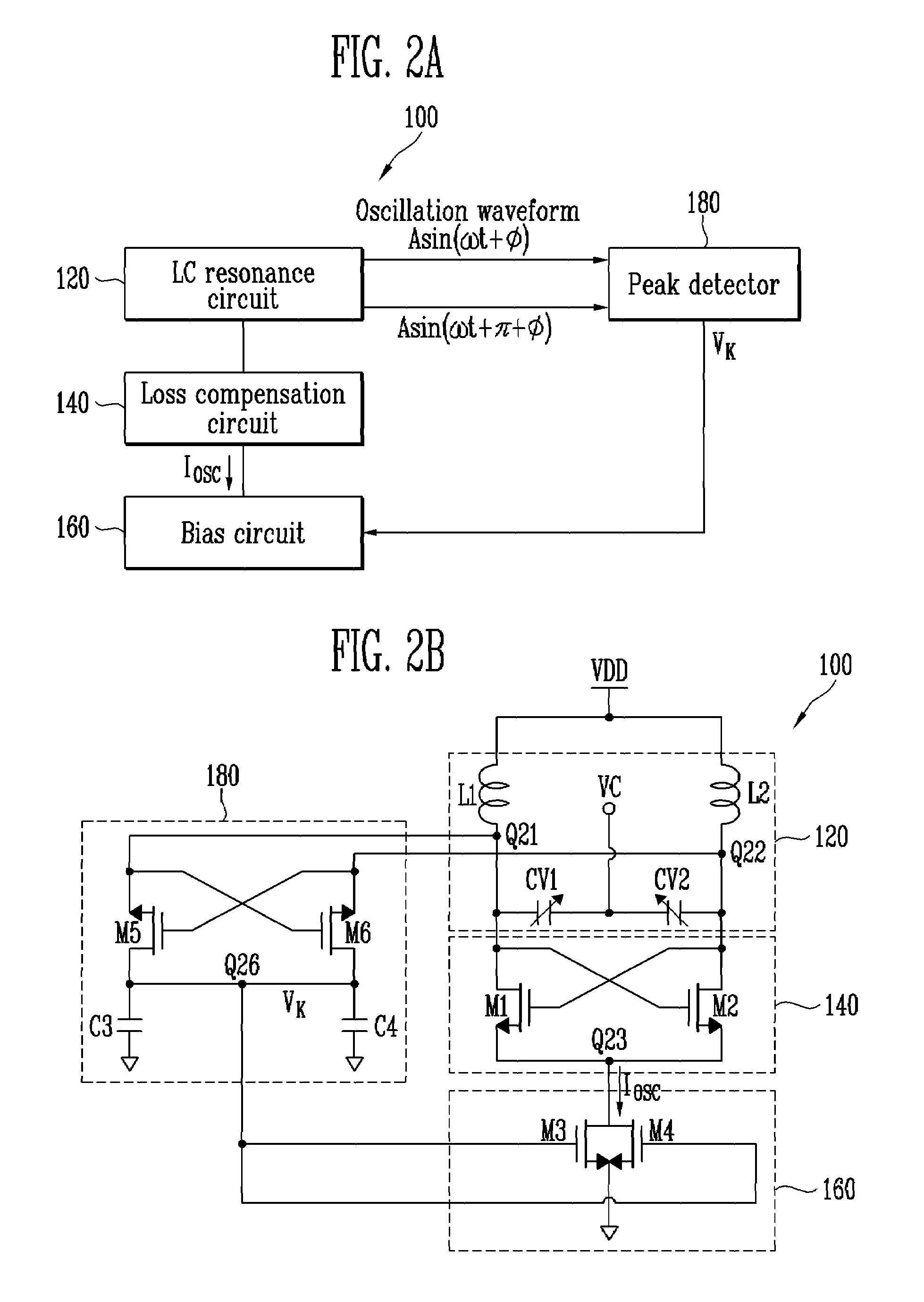
The present invention is about a voltage controlled oscillator that reduces flicker noise and improves phase noise characteristics. It achieves this by using a switching bias technique on a bias circuit. The invention also includes a common mode voltage that stabilizes the magnitude of the oscillation waveform with respect to changes in external conditions. The voltage controlled oscillator includes an LC resonance circuit, a loss compensation circuit, a bias circuit, and a peak detector. The peak detector applies the detected peak value from the oscillation waveform to the bias circuit, which then turns on / off the transistors in the bias circuit accordingly. The technical effects of the invention are reduced flicker noise, improved phase noise characteristics, and reduced chip area, making it easier to integrate.

Problems solved by technology

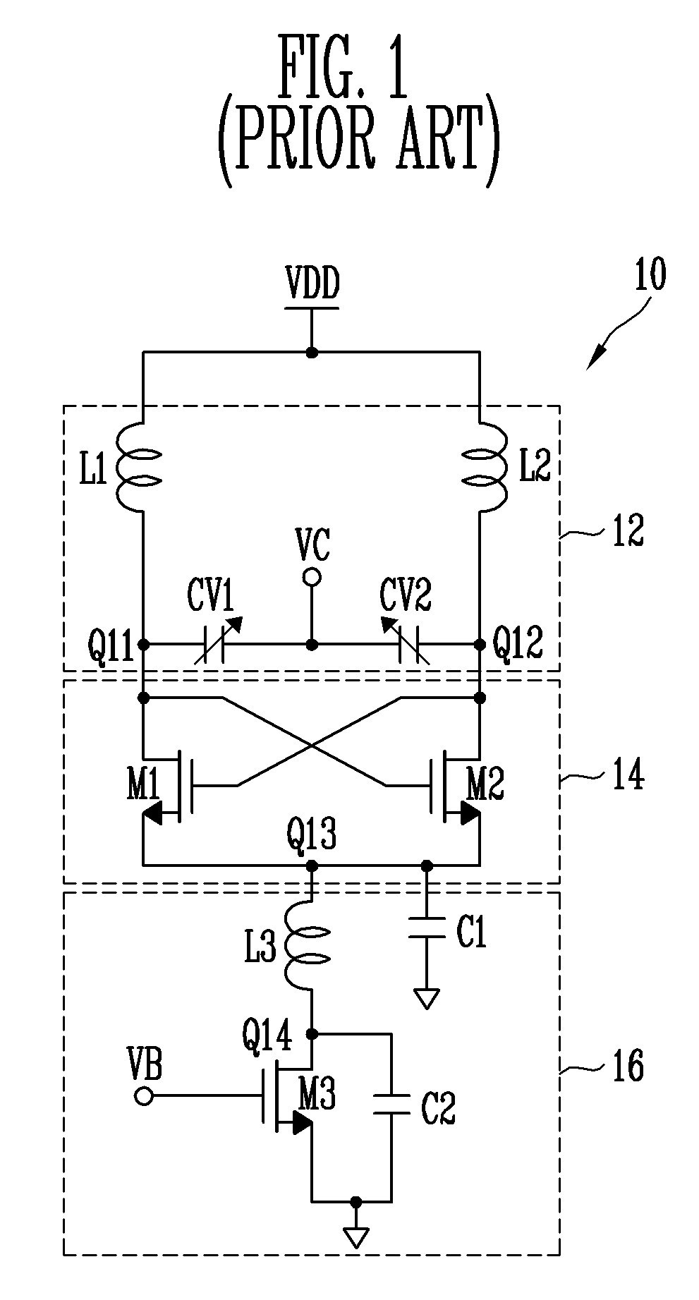
Therefore, when an integrated circuit is designed, a chip area inevitably increases.
Further, since the magnitude of the oscillation waveform significantly changes with respect to changes in external conditions, such as frequency tuning, a process change, a temperature change, and so on, the operation of the voltage controlled oscillator is unstabilized.

Method used


Image

  • Voltage controlled oscillator with switching bias
  • Voltage controlled oscillator with switching bias
  • Voltage controlled oscillator with switching bias

Examples


Embodiment Construction

[0028]Before the present invention is described, a research result will be briefly described. In the research, when a switching bias technique was used instead of applying a constant voltage to the gate terminal of a MOS transistor through which a bias current was flowed, flicker noise was lowered by 5-7 dB. The result of the research is disclosed in “MOSFET 1 / f Noise Measurement under Switched Bias Conditions” (IEEE Electron Device Letters, January, 2000) by A. P. van der Wel.

[0029]In the present invention, the switching bias technique is applied to a voltage controlled oscillator in accordance with the result of the above research. That is, an oscillation waveform of the voltage controlled oscillator is used for switching a bias circuit. Then, phase noise characteristics are enhanced, and the magnitude of the oscillation waveform is stabilized. Hereinafter, exemplary embodiments of the present invention will be described in detail with reference to the accompanying drawings.

[0030]...


PUM


Abstract

Provided is a voltage controlled oscillator to which a switching bias technique is applied so as to lower flicker noise of a bias circuit and enhance phase noise characteristics, thereby reducing the overall chip area to make it possible to achieve integration. A common mode voltage applied to the bias circuit is negatively fed back to an oscillation waveform. Therefore, it is possible to stabilize the magnitude of the oscillation waveform of the voltage controlled oscillator with respect to a change in an external condition.

Description

CROSS-REFERENCE TO RELATED APPLICATION[0001]This application claims priority to and the benefit of Korean Patent Application No. 2007-0042003, filed Apr. 30, 2007, the disclosure of which is incorporated herein by reference in its entirety.BACKGROUND[0002]1. Field of the Invention[0003]The present invention relates to a voltage controlled oscillator with a switching bias, and more specifically, to a voltage controlled oscillator to which a switching bias technique is applied so as to enhance phase noise characteristics and stabilize the magnitude of an oscillation waveform.[0004]The present invention is derived from a project entitled “Development of Digital RF and ADC Chips for Multi-Mode SDR Terminal [2006-S-015-01]” conducted as an IT R&D program for the Ministry of Information and Communication (Republic of Korea).[0005]2. Discussion of Related Art[0006]In general, a voltage controlled oscillator means an oscillator which changes the capacitance of a variable capacitor through v...

Claims


Application Information

Patent Timeline
Patent Type & Authority Patents(United States)
IPC IPC(8): H03L5/00
CPCH03B5/04H03L5/00H03B5/1228H03B5/1215H03B5/1243H03B5/12
Inventor MIN, BYUNG HUNKIM, YOUNG HOCHOI, BYOUNG GUNHYUN, SEOK BONG
Owner ELECTRONICS & TELECOMM RES INST
Learn More