Pattern forming apparatus
a technology of pattern forming and pattern, which is applied in the direction of turning machine accessories, drawing profiling tools, turning machines, etc., can solve the problems of high cost required for equipment for replacing optical paths with inert gas, high cost of lens materials, and long time for exposing a single piece of wafer, etc., to achieve high accuracy of alignment
- Summary
- Abstract
- Description
- Claims
- Application Information
AI Technical Summary
Benefits of technology
Problems solved by technology
Method used
Image
Examples
first embodiment
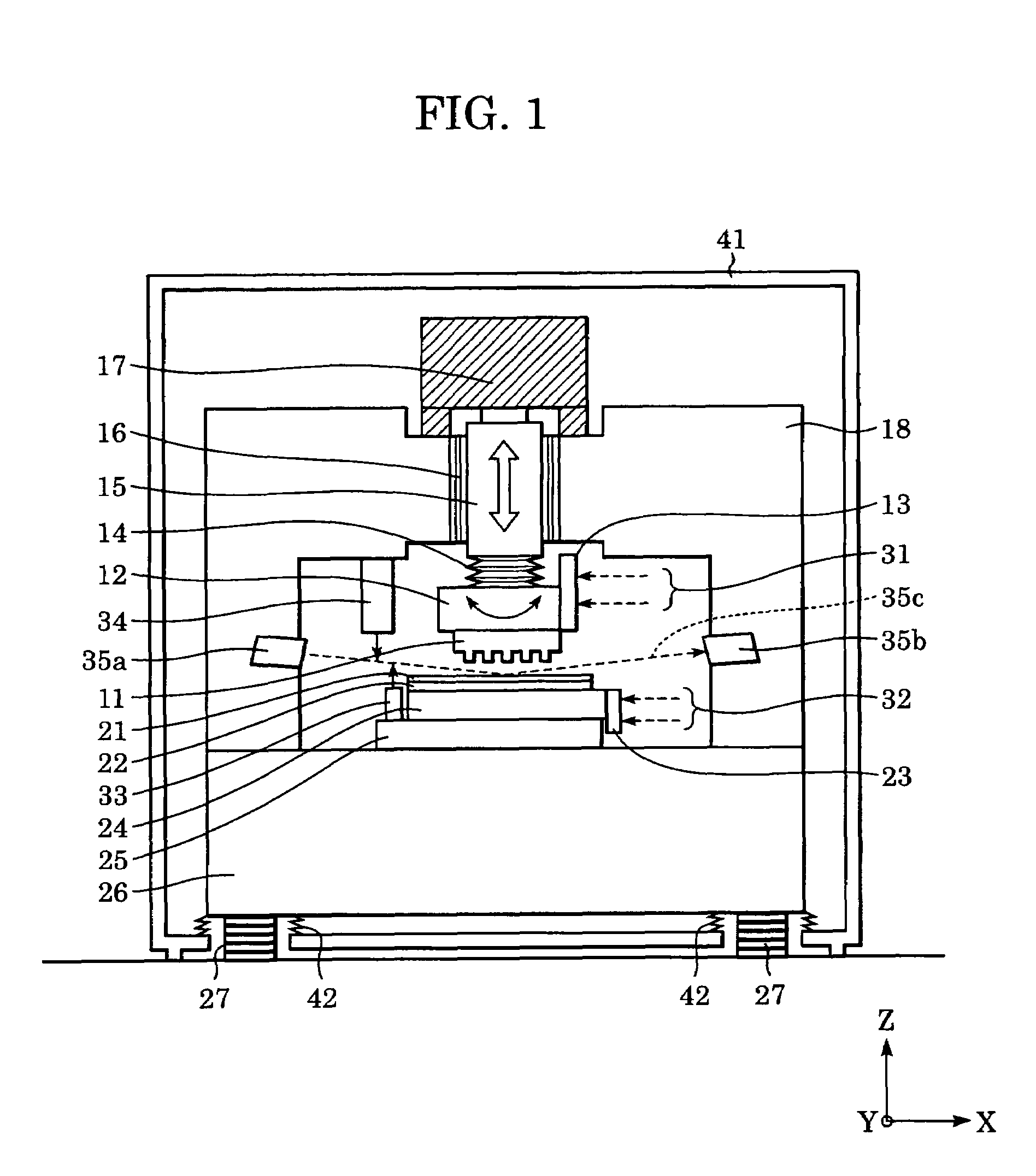
[0039]FIG. 1 is a drawing illustrating a pattern forming apparatus (nanoimprint apparatus) according to the present embodiment, showing a general structure of the apparatus. In order to facilitate the description, the directions are defined as shown by arrows in the drawing. The lateral direction is defined as X-axis, the perpendicular direction is defined as Y-axis, and the vertical direction is defined as Z-axis with respect to the plane of the drawing.
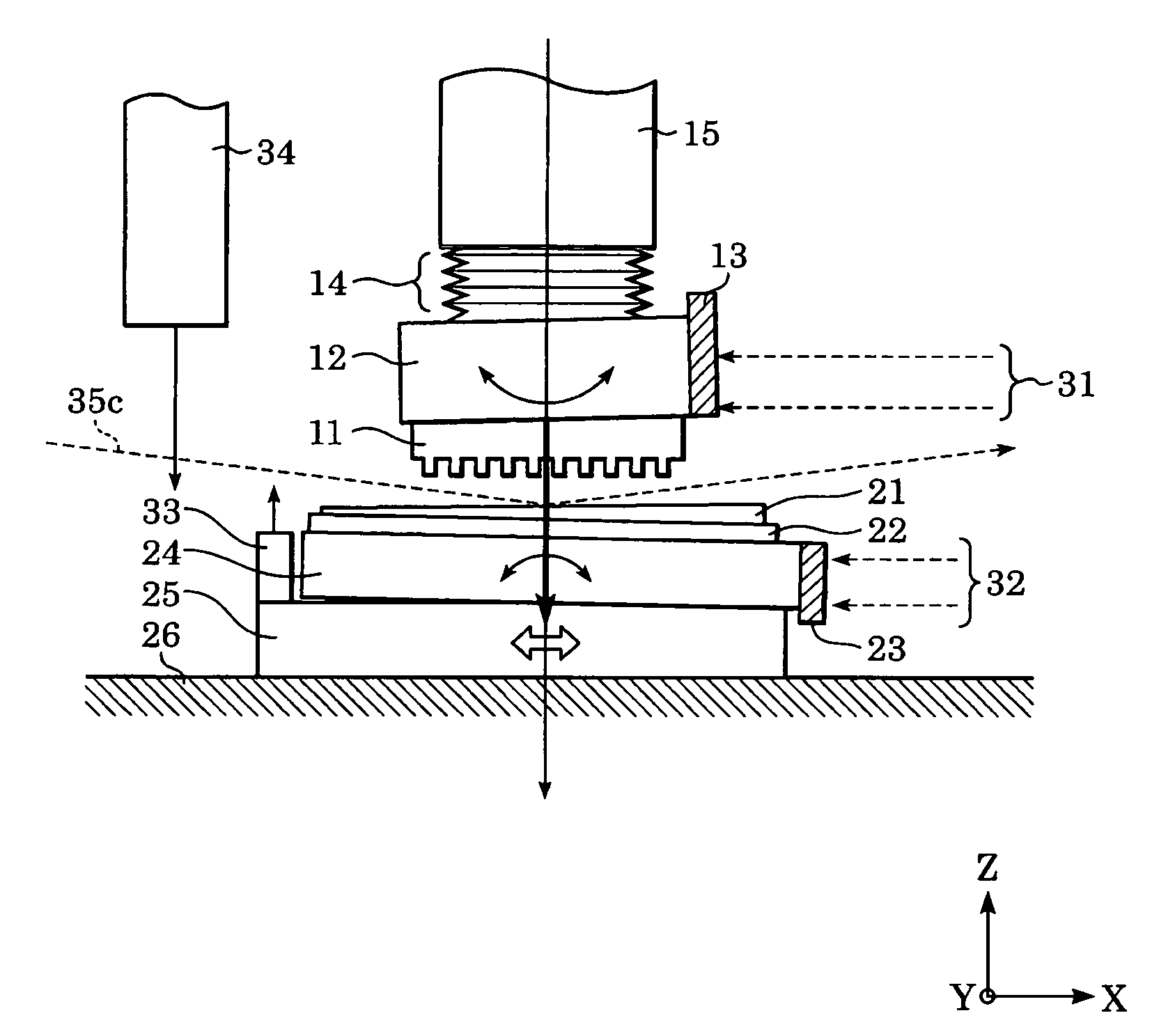
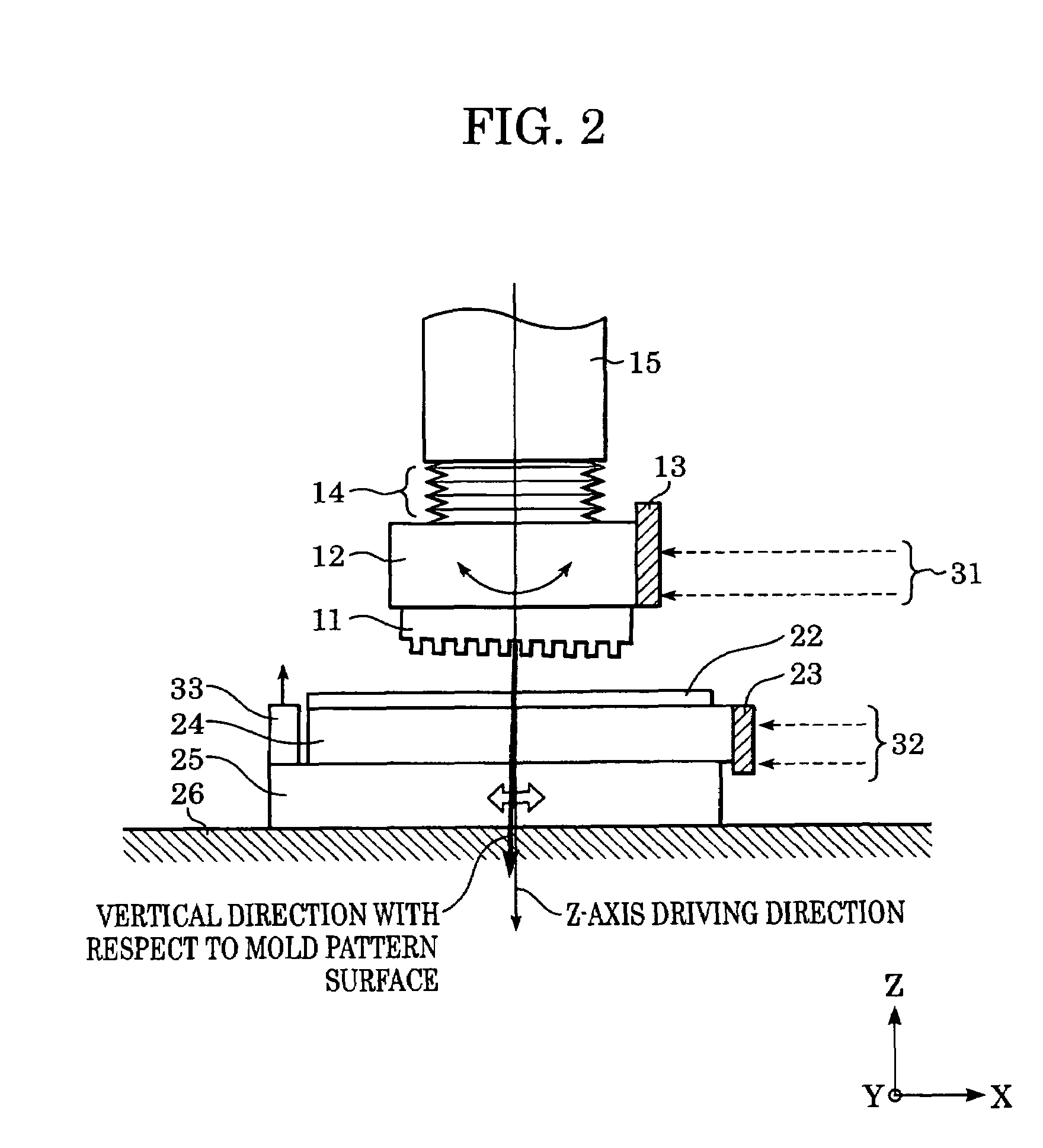
[0040]A mold 11 is an original plate and is formed with a fine pattern on the lower surface thereof by an Electron Beam Lithography or the like. The mold 11 is retained by a mold chuck 12 as a retaining device. The mold chuck 12 includes an electrostatic chuck for retaining an object with an electrostatic force and a mechanical chuck for retaining the object mechanically. A mold reference mirror 13 having extremely high level of flatness is fixed to the mold chuck 12, which serves as a measured section for position measurement and a...
second embodiment
[0069]FIG. 7 is a drawing illustrating the pattern forming apparatus (nanoimprint apparatus) according to the present embodiment, and showing a general structure of the entire apparatus. In order to facilitate the description, the directions are defined as shown by arrows in the drawing. The lateral direction is defined as X-axis, the perpendicular direction is defined as Y-axis, and the vertical direction is defined to Z-axis with respect to the plane of the drawing. The like reference member as in the first embodiment are represented by the same reference numerals.
[0070]The mold 11 is an original plate and is formed with a fine pattern on the lower surface thereof by an EB drawing apparatus or the like. The mold 11 is retained by a mold chuck 12 as a retaining device. The mold chuck 12 includes an electrostatic chuck for retaining an object with an electrostatic force and a mechanical chuck for retaining the object mechanically. A mold reference mirror 13 having extremely high lev...
third embodiment
[0100]Subsequently, an embodiment of a manufacturing method of a device utilizing the above-described fine processing apparatus will be described.
[0101]FIG. 15 shows a manufacturing flow of a semiconductor device (semiconductor chip such as an IC or LSI, a liquid crystal panel, a CCD, etc . . . . ). In Step 1 (circuit design), a circuit of the semiconductor device is designed. In Step 2 (mold manufacturing), a mold on which the designed circuit pattern is formed is manufactured. On the other hand, in Step 3 (wafer manufacturing), a wafer is manufactured using material such as silicon. Step 4 (wafer process) is referred to as preprocess, where an actual circuit is formed on the wafer using the prepared mold and the wafer. The subsequent Step 5 (assembly) is referred to as post-process, which is a process for obtaining chips using the wafer manufactured in Step 5 and includes an assembling step (dicing, bonding), a packaging step (encapsulation of the chip). In Step 6 (inspection), in...
PUM
| Property | Measurement | Unit |
|---|---|---|
| density | aaaaa | aaaaa |
| speed | aaaaa | aaaaa |
| wavelength | aaaaa | aaaaa |
Abstract
Description
Claims
Application Information
 - R&D
- Intellectual Property
- Life Sciences
- Materials
- Tech Scout
- Unparalleled Data Quality
- Higher Quality Content
- 60% Fewer Hallucinations
Browse by: Latest US Patents, China's latest patents, Technical Efficacy Thesaurus, Application Domain, Technology Topic, Popular Technical Reports.
© 2025 PatSnap. All rights reserved.Legal|Privacy policy|Modern Slavery Act Transparency Statement|Sitemap|About US| Contact US: help@patsnap.com


