Multi-component wavelength conversion devices and lasers incorporating the same

a wavelength conversion device and wavelength conversion technology, applied in the direction of laser details, instruments, light demodulation, etc., can solve the problems of image defects, reduce the conversion efficiency of the system, and the output wavelength of a semiconductor laser to move outside of this allowable bandwidth, so as to reduce the speckle effect of imag

Inactive Publication Date: 2010-01-19
CORNING INC
View PDF13 Cites 2 Cited by
  • Summary
  • Abstract
  • Description
  • Claims
  • Application Information

AI Technical Summary

Benefits of technology

[0003]The bandwidth of a PPLN SHG device is often very small—for a typical PPLN SHG wavelength conversion device, the full width half maximum (FWHM) wavelength conversion bandwidth is often only in the 0.16 to 0.2 nm range and mostly depends on the length of the crystal. Mode hopping and uncontrolled wavelength variations within the laser cavity due to change of the drive current can cause the output wavelength of a semiconductor laser to move outside of this allowable bandwidth during operation. Once the semiconductor laser wavelength deviates outside the wavelength conversion bandwidth of the PPLN SHG device, the output power of the conversion device at the target wavelength drops drastically. These changes in wavelength can be caused by several factors. For example, the DBR section temperature is affected by the amplitude of the gain-section drive current due to the thermal-crosstalk effect. There are other factors that make the DBR laser wavelength different from the PPLN wavelength, including variation of the ambient temperature and manufacturing tolerance of a DBR laser and a PPLN. In laser projection systems using a light source consisting of a DBR laser and a PPLN, for example, the wavelength fluctuations of the laser often generates some variation over time of the crystal conversion efficiency. This causes some variations of the frequency converted light which results in image defects that can be readily visible as defects at specific locations in the image. These visible defects typically manifest themselves as organized, patterned image defects across the image as well as pseudo random noise in the image. One method for minimizing those image artifacts consists of using crystals with larger spectral band pass. However, increasing the band pass by using shorter crystals, for example, typically decreases the conversion efficiency of the system. It is therefore often impossible to insure both low image noise and high system efficiency in the system.
[0007]In other embodiments of the present invention, the waveguide components are configured to define different phase matching wavelengths and the controller is programmed to allow for selection of an optimum phase matching wavelength or to execute a spectral bandwidth broadening mode by registering an optical signal propagating along the optical path with successive ones of the waveguide components. These modes of operation can be used to take advantage of a broader distribution of lasers in manufacturing, relieve some of the design constraints introduced when using tunable DBR lasers to achieve phase matching, or reduce image speckle in laser projection systems.

Problems solved by technology

Mode hopping and uncontrolled wavelength variations within the laser cavity due to change of the drive current can cause the output wavelength of a semiconductor laser to move outside of this allowable bandwidth during operation.
This causes some variations of the frequency converted light which results in image defects that can be readily visible as defects at specific locations in the image.
These visible defects typically manifest themselves as organized, patterned image defects across the image as well as pseudo random noise in the image.
However, increasing the band pass by using shorter crystals, for example, typically decreases the conversion efficiency of the system.
It is therefore often impossible to insure both low image noise and high system efficiency in the system.

Method used


Image

  • Multi-component wavelength conversion devices and lasers incorporating the same
  • Multi-component wavelength conversion devices and lasers incorporating the same
  • Multi-component wavelength conversion devices and lasers incorporating the same

Examples


Embodiment Construction

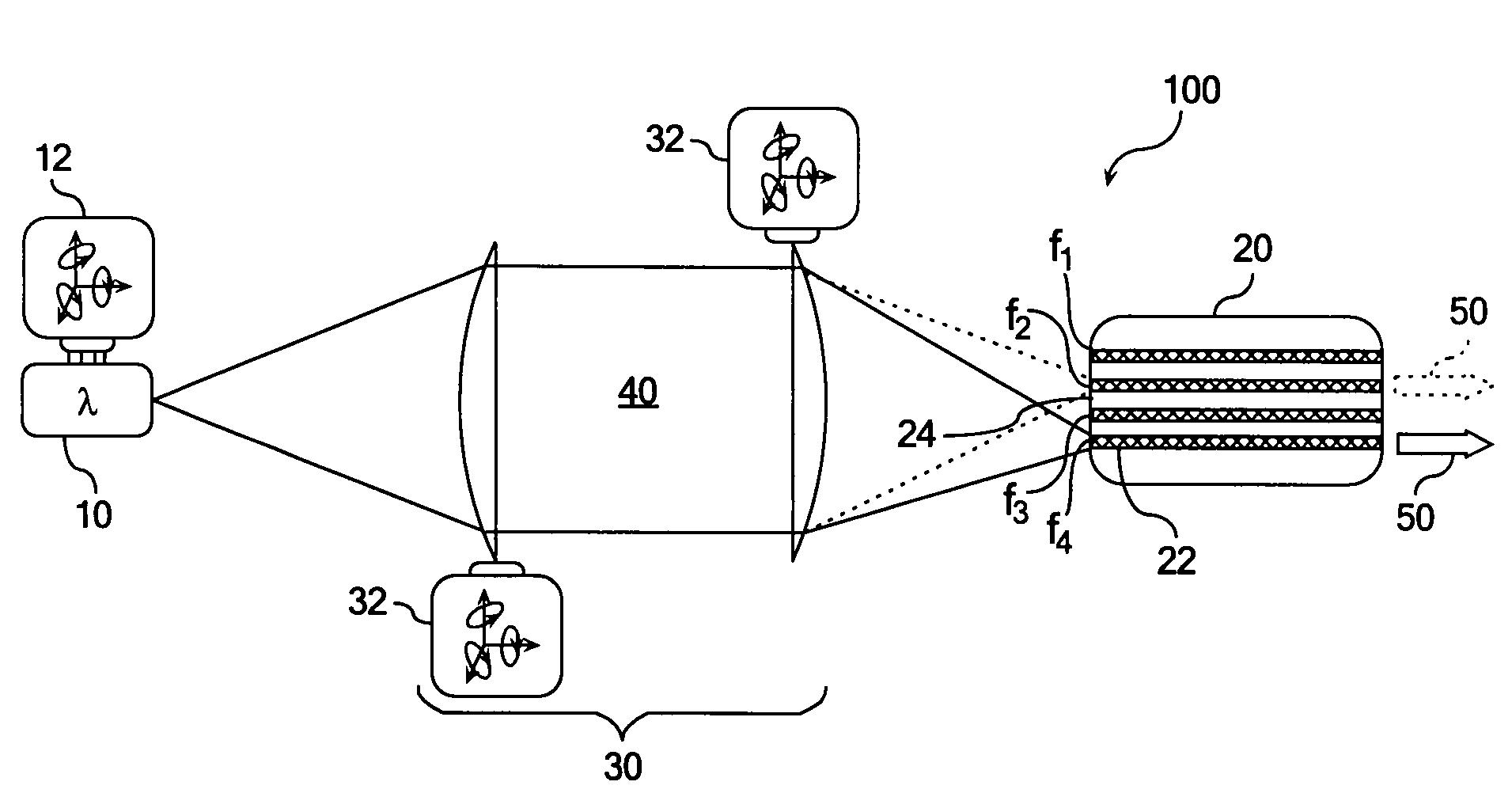
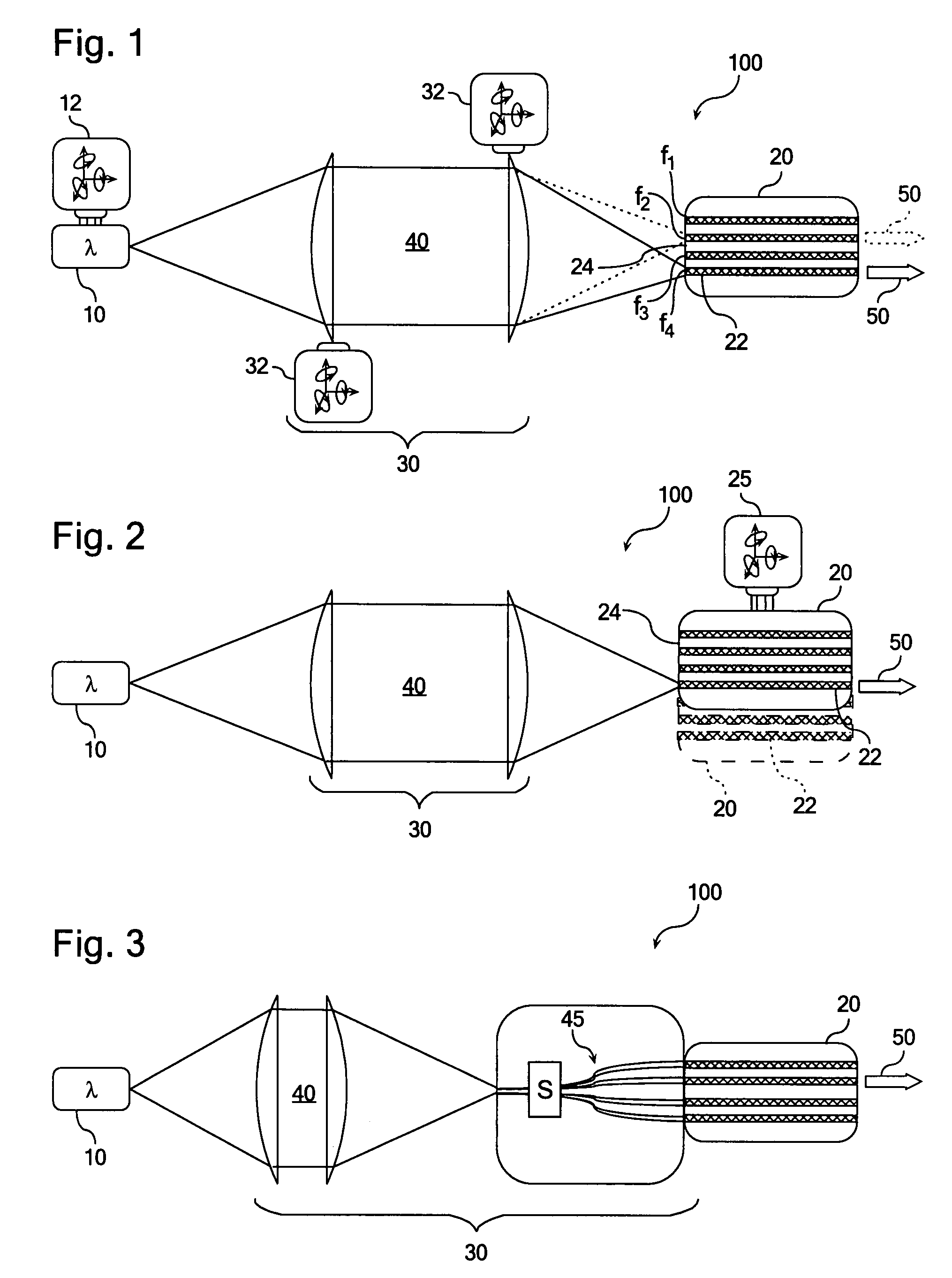
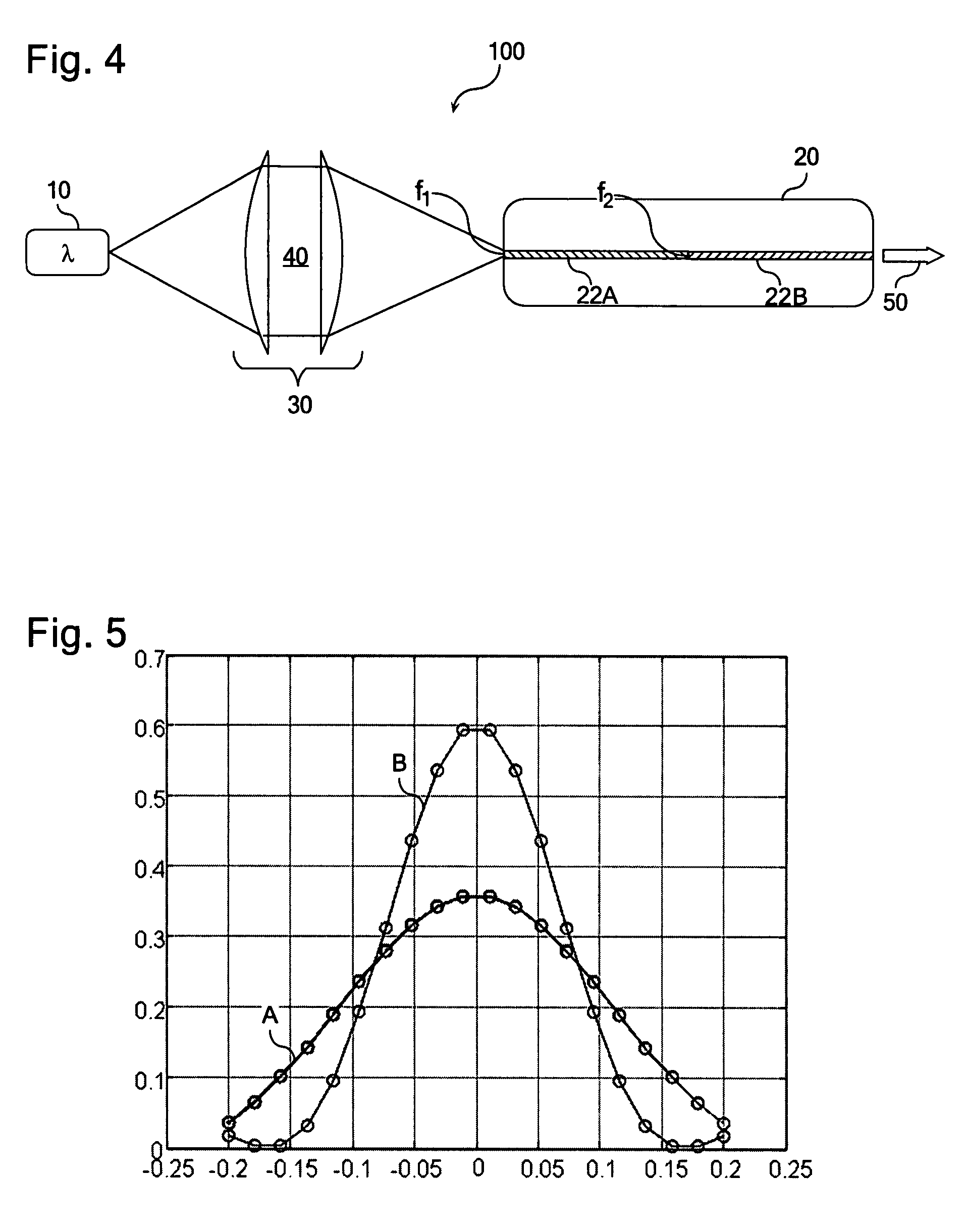
[0014]Referring initially to FIG. 1, a frequency-converted laser source 100 according to one embodiment of the present invention is illustrated. The laser source 100 comprises a laser 10, a wavelength conversion device 20, and coupling optics 30 positioned along an optical path 40 defined between the laser 10 and the wavelength conversion device 30. Typically, the wavelength conversion device 20 is configured as a monolithic PPLN SHG crystal, or other suitable wavelength conversion material. The wavelength conversion device 20 converts the incident light into higher harmonic waves and outputs a wavelength-converted signal 50. This type of configuration is particularly useful in generating shorter wavelength laser beams from longer wavelength semiconductor lasers and can be used, for example, as a visible laser for laser projection systems.

[0015]The wavelength conversion device 20 comprises a plurality of waveguide components 22 comprising respective input faces positioned in an effe...


PUM


Abstract

According to one embodiment of the present invention, a frequency-converted laser source is provided wherein the wavelength conversion device comprises a plurality of waveguide components comprising respective input faces positioned in an effective focal field of the laser source. Individual ones of the waveguide components contribute different elements to a set of distinct wavelength conversion properties, defining a set of distinct wavelength conversion properties attributable to the waveguide components. The set of distinct wavelength conversion properties comprises properties representing phase matching wavelengths of the waveguide components, spectral widths of the waveguide components, conversion efficiency of the waveguide components, or combinations thereof. Additional embodiments are disclosed and claimed.

Description

BACKGROUND OF THE INVENTION[0001]The present invention relates generally to semiconductor lasers, laser controllers, laser projection systems, and other optical systems incorporating semiconductor lasers. More particularly, by way of illustration and not limitation, embodiments of the present invention relate generally to the use of wavelength conversion devices in optical packages, laser projection systems, and other optical systems incorporating semiconductor lasers.SUMMARY OF THE INVENTION[0002]Short wavelength sources can be configured for high-speed modulation by combining a single-wavelength semiconductor laser, such as a distributed feedback (DFB) laser, a distributed Bragg reflector (DBR) laser, or a Fabry-Perot laser with a wavelength conversion device, such as a second harmonic generation (SHG) crystal. The SHG crystal can be configured to generate higher harmonic waves of the fundamental laser signal by tuning, for example, a 1060 nm DBR or DFB laser to the spectral cente...

Claims


Application Information

Patent Timeline
Patent Type & Authority Patents(United States)
IPC IPC(8): H01S3/10H01S5/00
CPCG02F1/3532G02F2201/18G02F2203/58H01S5/005H01S5/0071H01S5/0092
Inventor GOLLIER, JACQUESHARRIS, JAMES MICHEAL
Owner CORNING INC
Why Eureka
Try Eureka