
Transparent material processing with an ultrashort pulse laser

a technology transparent material, which is applied in the field of ultrashort pulse laser processing, can solve the problems of poor cleave process precision, low quality of cleave facets, and additional interaction, and achieve the effects of reducing the degree of localization of weld features, reducing the thickness of the material through which the beam can be focused, and increasing linear absorption

Inactive Publication Date: 2009-12-01
IMRA AMERICA
View PDF73 Cites 62 Cited by
  • Summary
  • Abstract
  • Description
  • Claims
  • Application Information

AI Technical Summary

Benefits of technology

This patent describes a method for using ultrashort laser pulses to create patterns in transparent materials. The laser pulses can create surface grooves and internal interfaces within the material, resulting in optical waveguides and optical defects that can scatter light. The method allows for faster and more precise cleaving of the material, with no need for a surface scribe line. The patterns created can be used for indicators or as value-added features in the material. The method also allows for controlled illumination of the patterns for increased visibility or reduced visibility depending on the application. Overall, the method provides a faster and more precise way to modify and bond transparent materials.

Problems solved by technology

The high repetition rate of the laser and significant pulse-to-pulse overlap results in an additional interaction between the material modification created by the previous laser exposure and the subsequent pulses in the same region.
If the surface groove is too shallow, the fracture will tend to wander, resulting in low quality cleave facets and poor cleave process precision.

Method used


Image

  • Transparent material processing with an ultrashort pulse laser
  • Transparent material processing with an ultrashort pulse laser
  • Transparent material processing with an ultrashort pulse laser

Examples


Embodiment Construction

[0067]1. Ultrashort Pulse Laser Scribing

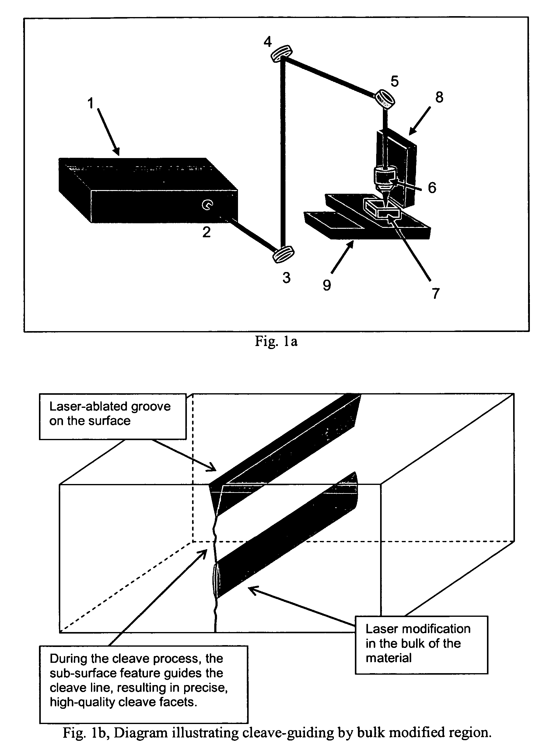
[0068]FIG. 1 illustrates one embodiment of the current invention, which is a method for scribing transparent materials for subsequent cleaving. This embodiment employs a laser system (1) producing a beam of ultrashort laser pulses (2), an optical system (6) that generates a desired laser beam intensity distribution, and a target material (7) to be scribed that is transparent to the wavelength of the laser pulses. In addition, a Z-axis stage (8) is used for beam focus position control (depth), and an automated X-Y axis stage assembly (9) is generally required for moving the work pieces (7) laterally relative to the focused laser beam. Alternatively, the laser beam (2) could be moved relative to a stationary target material with the use of scanning mirrors (3), (4), and (5).

[0069]The laser beam (2) is directed through the optical system (6), which transforms the laser beam (2) to create a desired 3-dimensional intensity distribution. Particular ...


PUM

PropertyMeasurementUnit
melting temperatureaaaaaaaaaa
distanceaaaaaaaaaa

Abstract

Methods for ultrashort pulse laser processing of optically transparent materials. A method for scribing transparent materials uses ultrashort laser pulses to create multiple scribe features with a single pass of the laser beam across the material, with at least one of the scribe features being formed below the surface of the material. This enables clean breaking of transparent materials at a higher speed than conventional techniques. Slightly modifying the ultrashort pulse laser processing conditions produces sub-surface marks. When properly arranged, these marks are clearly visible with side-illumination and not clearly visible without side-illumination. In addition, a method for welding transparent materials uses ultrashort laser pulses to create a bond through localized heating. The ultrashort pulse duration causes nonlinear absorption of the laser radiation, and the high repetition rate of the laser causes pulse-to-pulse accumulation of heat within the materials. The laser is focused near the interface of the materials, generating a high energy fluence at the region to be welded. This minimizes damage to the rest of the material and enables fine weld lines.

Description

BACKGROUND OF THE INVENTION[0001]1. Field of the Invention[0002]This invention relates to ultrashort pulse laser processing of optically transparent materials, including material scribing, welding and marking.[0003]2. Description of the Related Art[0004]A. Cutting and Scribing[0005]Cutting of optically transparent materials is often done with mechanical methods. Perhaps the most common method for cutting thin, flat materials is using a mechanical dicing saw. This is the standard method in the microelectronics industry for dicing silicon wafers. However, this method generates significant debris that must be managed in order to avoid parts contamination, resulting in increased overall cost of the process. In addition, the thinner wafers being used for advanced microprocessor designs tend to shatter when cut with a dicing saw.[0006]To address these problems, current state-of-the-art processes for “scribe and cleave” material cutting use various types of lasers to scribe a surface groov...

Claims


Application Information

Patent Timeline
Patent Type & Authority Patents(United States)
IPC IPC(8): B23K26/00
CPCB23K26/0617B23K26/246B23K26/367B23K26/4075B28D5/0011B29C65/1635B29C65/1658B29C66/1122B29C66/3282B29C66/43B29C66/71B29C66/73366B29C66/90C03B23/20C03B23/203B23K26/0635B29C65/14B81B1/00B29C66/934B29C59/16C03B33/0222B23K26/0057B29C66/41B29C66/836B29C66/91641Y10T428/15B29C65/1616B29C65/1638B29C65/1696B29C65/38B29C66/30223B29C66/322B29C66/7352B29C66/919B29C66/939B29C66/949B29K2033/12B29K2069/00B29K2995/0026Y10T428/24802B29C65/1664B29C65/1674B29C66/944Y10T428/13Y10T428/24479B29C65/00B23K26/40B29C66/73921B23K26/0624B23K26/244B23K26/364B23K26/53B23K2103/50C03C23/0025B81C1/00119
Inventor BOVATSEK, JAMESARAI, ALAN Y.YOSHINO, FUMIYO
Owner IMRA AMERICA
Learn More