Electronic component module
a technology of electronic components and components, applied in the direction of printed circuits, sustainable manufacturing/processing, final product manufacturing, etc., can solve the problems of limiting the amount of bonding strength and the limiting amount of shock resistance that can be improved, so as to improve the shock resistance and the effect of less likely to be damaged
- Summary
- Abstract
- Description
- Claims
- Application Information
AI Technical Summary
Benefits of technology
Problems solved by technology
Method used
Image
Examples
first preferred embodiment
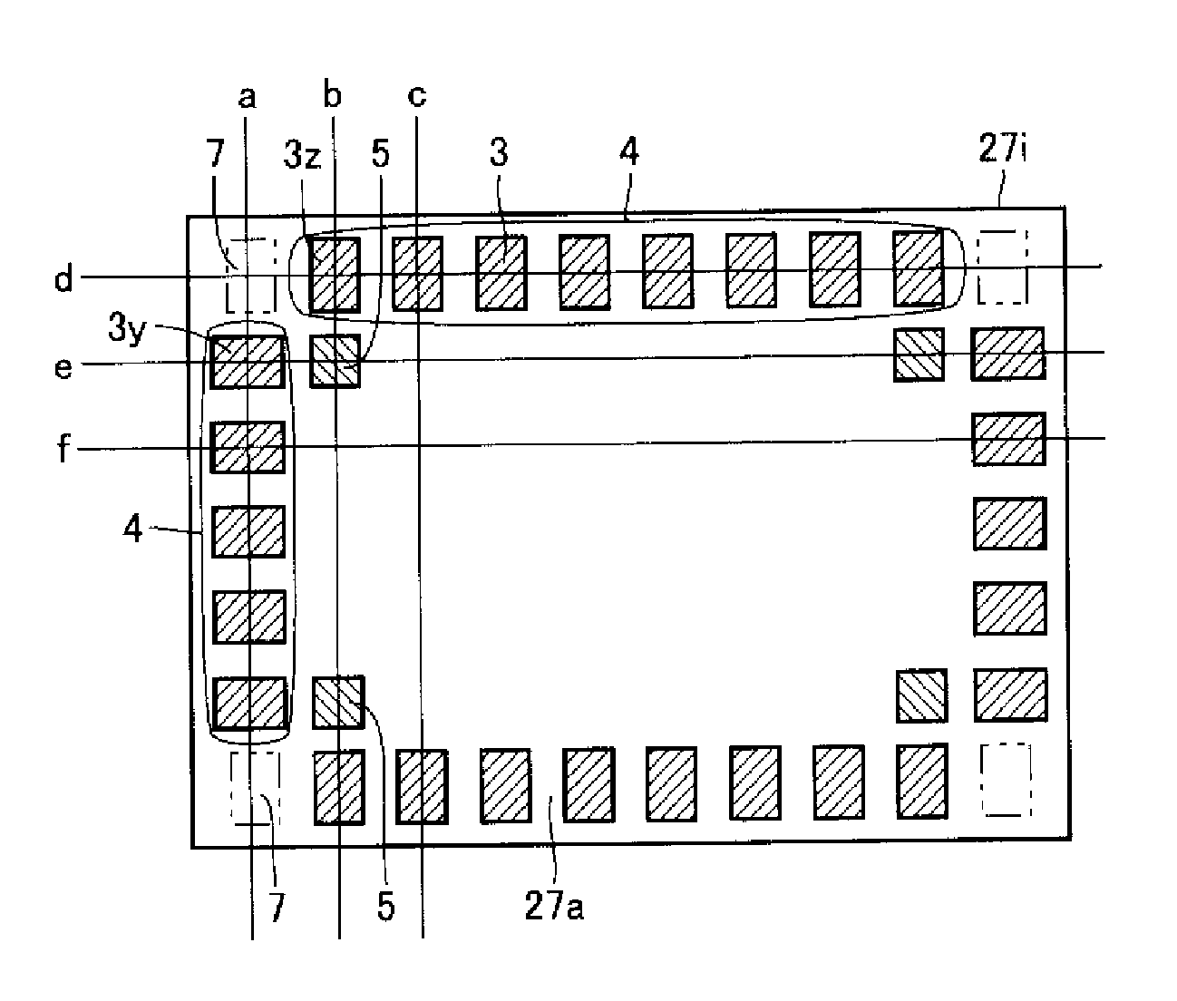
[0025]An electronic component module in a first preferred embodiment according to the present invention will be described with reference to FIG. 1. FIG. 1 shows the rear surface 27a of the electronic component module 27i, that is, the surface on which soldering lands are arranged. The electronic component module 27i is an electronic component module that is provided with a ceramic substrate and a plurality of soldering lands 3. The ceramic substrate has the rear surface 27a preferably having a substantially rectangular shape. The plurality of soldering lands 3 are arranged on the rear surface 27a. The plurality of soldering lands 3 include outer peripheral land rows 4. Each of the outer peripheral land rows 4 is arranged in a line along each side of the rear surface 27a with the exception of corner portions 7 of the rear surface 27a. The corner portions 7 are areas in which no lands are present. However, lands are arranged in the areas of the corner portions 7 according to the known...
second preferred embodiment
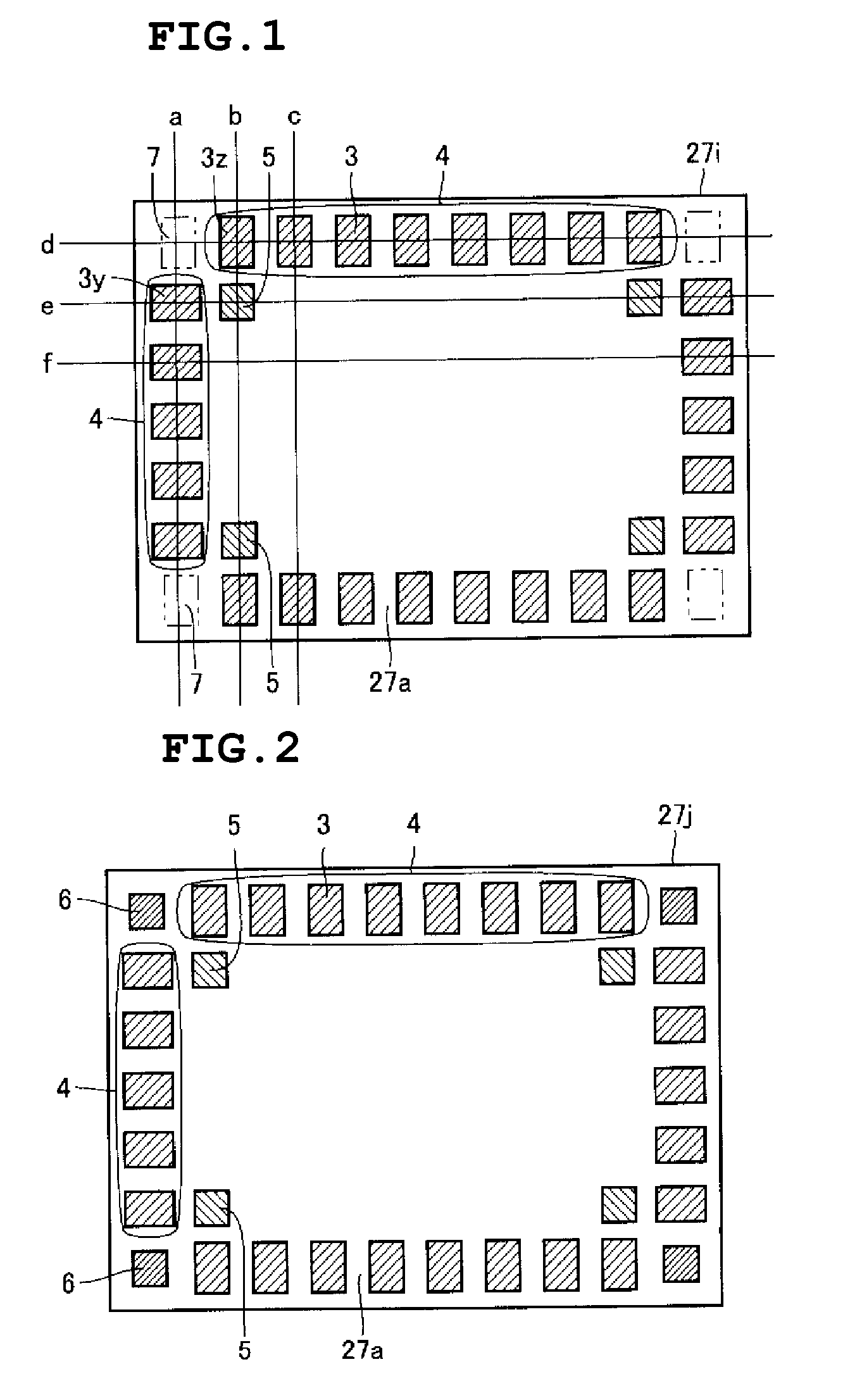
[0035]An electronic component module in a second preferred embodiment according to the present invention will be described with reference to FIG. 2. FIG. 2 shows the rear surface 27a of the electronic component module 27j. The electronic component module 27j is provided with the following structure in addition to the structure described in the first preferred embodiment. That is, non-soldering lands 6 are arranged at the corner portions of the rear surface 27a. The non-soldering lands 6 are lands that need not be soldered when the electronic component module 27j is mounted on the motherboard. For example, testing lands correspond to the non-soldering lands 6. The term “testing land” is a land that is electrically connected to a wiring pattern provided on the front surface or inside of the ceramic substrate for testing its electrical characteristics.
[0036]In this preferred embodiment, lands are arranged at the corner portions 7. However, the lands are not the soldering lands 3, and i...
third preferred embodiment
[0041]An electronic component module of a third preferred embodiment according to the present invention will be described with reference to FIG. 8. FIG. 8 shows the rear surface 27a of the electronic component module 27k. The electronic component module 27k is provided with the following structure in addition to the structure described in the first and second preferred embodiments. That is, the electronic component module 27k includes one or more short side inner land rows 8 that are arranged in lines along each short side of the substantially rectangular rear surface 27a and adjacent to the inner side of the outer peripheral land row 4.
[0042]In this preferred embodiment, because the bonding area may be increased between the electronic component module 27k and the motherboard, while avoiding stress concentration at the corner portions, shock resistance is enhanced.
[0043]The short side inner land row 8 may be arranged on only one of the short sides. However, it is preferable that the...
PUM
 Abstract
Description
Claims
Application Information
 - R&D
- Intellectual Property
- Life Sciences
- Materials
- Tech Scout
- Unparalleled Data Quality
- Higher Quality Content
- 60% Fewer Hallucinations
Browse by: Latest US Patents, China's latest patents, Technical Efficacy Thesaurus, Application Domain, Technology Topic, Popular Technical Reports.
© 2025 PatSnap. All rights reserved.Legal|Privacy policy|Modern Slavery Act Transparency Statement|Sitemap|About US| Contact US: help@patsnap.com


