Measurement of thin films using fourier amplitude

a technology of amplitude and measurement method, applied in the direction of phase-affecting property measurement, measurement device, instruments, etc., can solve the problem of changing the phase of multiple reflections in the film extremely quickly, and achieve the effect of more repeatability and robust results

Active Publication Date: 2009-11-03
BRUKER NANO INC
View PDF5 Cites 20 Cited by
  • Summary
  • Abstract
  • Description
  • Claims
  • Application Information

AI Technical Summary

Benefits of technology

[0010]As mentioned, a serious problem with the prior-art Fourier-phase approach resides in the fact that, as the thickness of the film is reduced, the phase of the multiple reflections in the film changes extremely quickly and, at some point (at about 0.1 micron or so), the phase to be measured is a small quantity (on the order of 0.01 to 0.02 radians—or 0.003 of a wavelength). Since the Fourier amplitude of a white-light interferogram spectrum (unlike its Fourier phase component) is a smooth function of wavelength, even for ultra-thin films the amplitude produces significantly more repeatable and robust results based on the same experimental procedure. Therefore, this problem is overcome by the Fourier-amplitude approach of the invention, which enables repeatable measurements of thickness of ultra-thin films on the order of about 0.1 micron. In particular, the method of the invention is expected to perform strongly even with extremely thin films (less than 0.1 micron). Additionally, unlike the prior-art approach, the method of the invention does not require initial guesses about the profile of the substrate surface.

Problems solved by technology

As mentioned, a serious problem with the prior-art Fourier-phase approach resides in the fact that, as the thickness of the film is reduced, the phase of the multiple reflections in the film changes extremely quickly and, at some point (at about 0.1 micron or so), the phase to be measured is a small quantity (on the order of 0.01 to 0.02 radians—or 0.003 of a wavelength).

Method used


Image

  • Measurement of thin films using fourier amplitude
  • Measurement of thin films using fourier amplitude
  • Measurement of thin films using fourier amplitude

Examples


Embodiment Construction

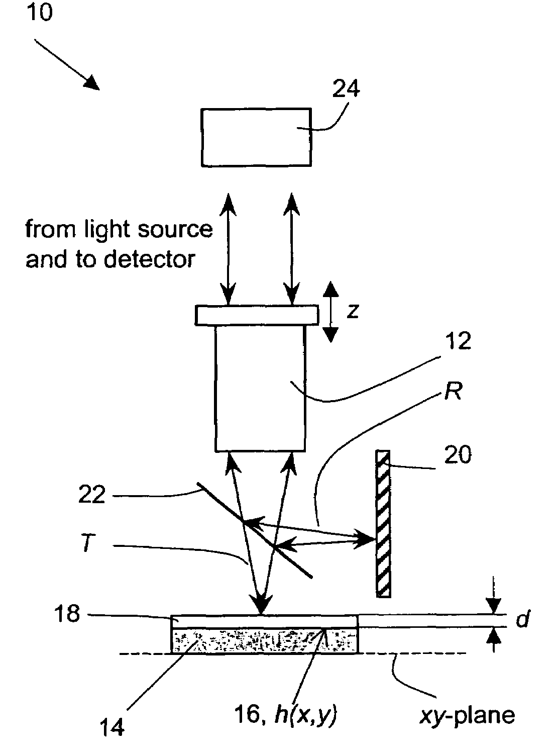
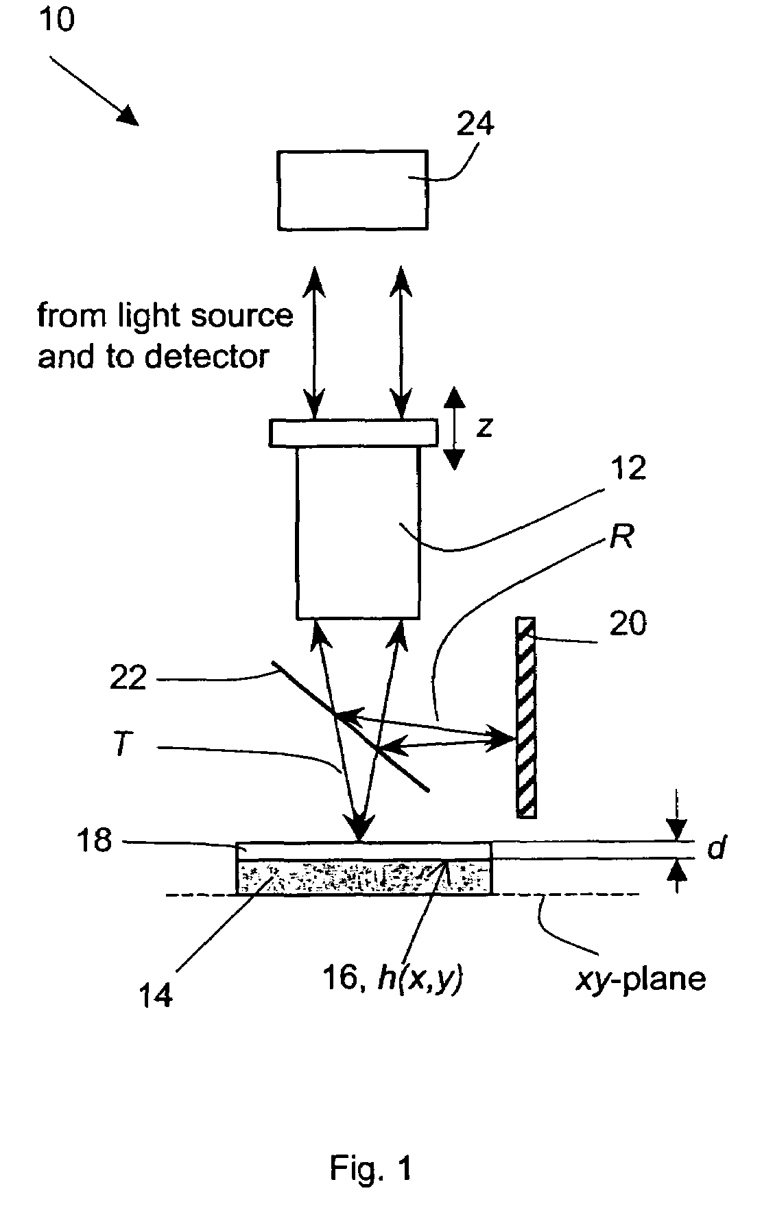
[0020]It is understood that the invention may be practiced with any conventional scanning interferometer, such as a Michelson, Mireau, or Linnik interferometer. The basic schematic configuration of a Michelson scanning interferometer 10 is illustrated for example in FIG. 1. An actuator (not shown) moves the objective 12 of the interferometer along the z axis (typically vertical) with respect to a test substrate 14 located on a stage (not shown) in the xy plane (typically horizontal). Alternatively, the substrate under test may be moved relatively to the objective. The test surface 16 of the substrate 14 has a profile h(x,y) and may be uncoated or coated with a thin film 18 of thickness d. A reference mirror 20 and a beam splitter 22, dividing the incident light received from the light source (not shown) into reference and test beams R and T, respectively, are positioned in front of the objective 12. The resulting white-light interferogram measured by a detector 24 is a low-coherence...


PUM


Abstract

Thin-film thickness and refractive index are measured using the Fourier amplitude of a broadband interferometric spectrum. Due to the smooth nature of the Fourier amplitude as a function of wavelength, as compared to the fast varying Fourier phase conventionally used to measure thickness, increased stability and repeatability of measurement are achieved. As a result, measurements of ultra-thin films with thickness below 100 nm are possible with reliable results.

Description

BACKGROUND OF THE INVENTION[0001]1. Field of the Invention[0002]This invention relates in general to techniques for measuring the characteristics of thin films. In particular, it relates to white-light scanning interferometric methods and systems for measuring the thickness of transparent thin-film coatings.[0003]2. Description of the Related Art[0004]White-light scanning interferometers (WLSIs) have gained popularity in opto-electronic industry for testing that goes beyond measuring the thickness of various elements of opto-electronic circuitry. The measurement technique of white-light scanning interferometry produces a short coherence interferogram that enables the measurement of the optical path difference between test and reference beams without 2π ambiguity. Unlike other conventional techniques, such as ellipsometry or spectroscopy, which cannot measure surface profile, this interferometric technique can produce both thickness and surface profile measurements of a transparent o...

Claims


Application Information

Patent Timeline
Patent Type & Authority Patents(United States)
IPC IPC(8): G01B11/02
CPCG01B11/0675G01N21/45G01N21/8422G01B9/02072G01B9/0209G01B9/02084G01B9/02057
Inventor WAN, DER-SHEN
Owner BRUKER NANO INC
Why Eureka
Try Eureka