Semiconductor integrated circuit device

a technology of integrated circuits and semiconductors, applied in the direction of power consumption reduction, pulse techniques, instruments, etc., can solve the problems of increasing design time and design errors, complex body bias control, and increasing the complexity of circuit modules to be arranged within the chip, so as to reduce the subthreshold leakage current, reduce power consumption performance, and improve the effect of speed performan

Inactive Publication Date: 2009-11-03
RENESAS ELECTRONICS CORP +1
View PDF11 Cites 25 Cited by
  • Summary
  • Abstract
  • Description
  • Claims
  • Application Information

AI Technical Summary

Benefits of technology

[0007]In order to implement a CMOS semiconductor integrated circuit device capable of both higher speed performance and lower power consumption performance at the same time, it is effective to perform body bias control to the CMOS circuit as described above. During stoppage of the CMOS circuit like the standby state or in a mode in which a low-speed operation can be performed, the body bias is deepened, whereby the threshold voltage of the MOS transistor is raised to thereby reduce the subthreshold leakage current, thus making it possible to reduce the power consumption. In the active state in which the CMOS circuit is performing a normal operation, the threshold voltage is lowered to thereby speed up operation. As a method for lowering the threshold voltage, there is known, in addition to the previously-described method, a method for setting the body bias to lower voltage than the supply voltage vdd for the pMOS transistor, and to voltage higher than the ground voltage gnd for the nMOS transistor (this operation will be referred to as “body bias will be made shallow” or “body bias will be made into a forward bias” hereinafter), or a method for supplying an optimum body bias in response to variations and the like in the transistor manufacturing process, or the like.
[0009]If a circuit block to be requested in order to control the body bias could be freely arranged outside a circuit module constituting the microprocessor, it would become possible to use the existing module without increasing the burden of designing the circuit module, thus making it possible to achieve optimum body bias control for each circuit module, and to implement higher performance of the chip and lower power consumption.
[0011](1) Even when the size and type of the circuit within the chip of the semiconductor integrated circuit to be constructed of the CMOS circuit such as the microprocessor are complicated and diverse, it is possible to design each circuit module without regard to the body bias control, and it becomes possible to shorten the design time and to improve the reliability.(2) Even when utilizing the existing circuit module, it becomes possible to use it for design without regard to the body bias control, resulting in shortened design time and improved reliability.(3) Even when combining circuit modules in diversified ways like ASIC, it is possible to design without regard to the body bias control, likewise enabling shortened design time and improved reliability.(4) Arbitrary body bias control is rendered possible for each circuit module within the chip, whereby higher speed of the processor and the like and lower power consumption will be realized.

Problems solved by technology

Incidentally, in the semiconductor integrated circuit devices in recent years, a number of transistors to be integrated on one chip or the size of the circuit has become enormous, and the circuit modules to be arranged within the chip have also become complicated and diverse.
As the structure of the interior of the chip becomes complicated as described above, body bias control also becomes complicated.
As a result, an increase in the load of considering the body bias control when designing the circuit module leads to an increase in design time and an increase in design errors.
Also, when an attempt is made to re-utilize an existing circuit module on designing a new semiconductor integrated circuit device, the existing module also may not be of module structure corresponding to the desired body control system.
For this reason, even though the body bias control to details is going to be made in response to complicated processor chip and trend toward multifunction of the module within the chip, the disadvantages that the load of designing increases and that the existing circuit module cannot be used arise, which possibly results in making it difficult to achieve the desired performance and reduce electric power.

Method used


Image

  • Semiconductor integrated circuit device
  • Semiconductor integrated circuit device
  • Semiconductor integrated circuit device

Examples


Embodiment Construction

[0040]Hereinafter, with reference to the drawings, the description will be made of the present invention.

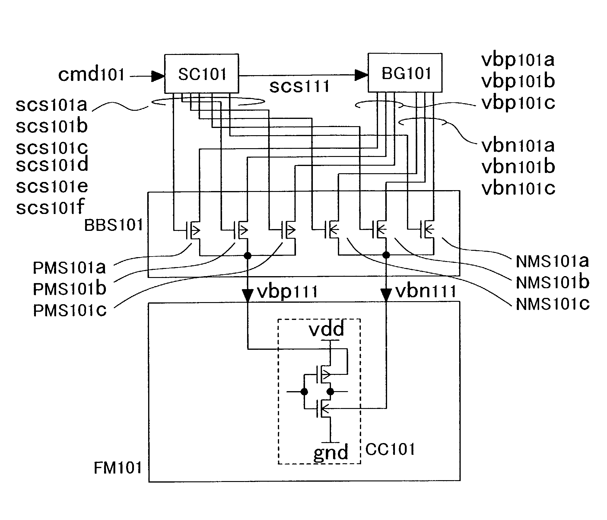
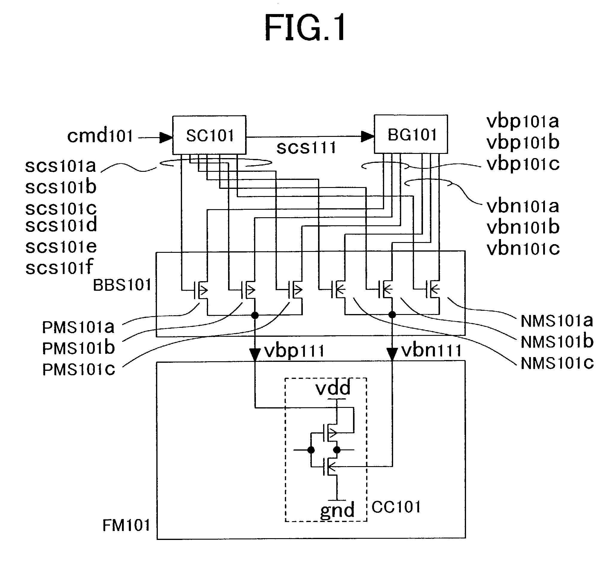
[0041]FIG. 1 is a view showing the first structural example of the present invention.

[0042]A semiconductor integrated circuit device according to the present embodiment is composed of: a functional module FM101 constituting a semiconductor integrated circuit such as a microprocessor consisting of a CMOS circuit; a switch controller SC101; a bias generator BG101; and a body bias switch circuit BBS101. The functional module FM101 consists of the CMOS circuit CC101. The body bias switch circuit BBS101 is constructed of pMOS transistors PMS101a-101c and nMOS transistors NMS101a-101c. The switch controller SC101 receives an instruction signal cmd101 to output a bias control signal scs111 to the bias generator BG101 and switch control signals scs101a to 101f to the bias switch circuit BBS101. The bias generator BG101 outputs, in response to the bias control signal scs111, body biases v...


PUM


Abstract

A body bias control system allows for independent design of a functional module, thereby reducing the burden of designing the module. The body bias control system provides a switch circuit having an area in which the body bias is controlled independently of its outside portion, for controlling the supply of body bias in the vicinity of the area. Preferably three types of switches are provided for switching the body bias to suitable levels for a standby mode, a mode of normal operation and a mode of high-speed operation.

Description

BACKGROUND OF THE INVENTION[0001]1. Field of the Invention[0002]The present invention relates to a semiconductor integrated circuit device, and more particularly to a semiconductor integrated circuit device for achieving high speed and low power consumption at the same time.[0003]2. Description of Related Art[0004]High speed performance and the low power consumption are demanded of a semiconductor integrated circuit device using a CMOS circuit. Particularly, in the CMOS circuit to be used in a battery-driven device such as a portable information apparatus, since it becomes possible to extend the battery life by reducing the power consumption, manufacturers have demanded that the power consumption be reduced. The power consumption of the CMOS circuit includes dynamic power consumption associated with charging / discharging current during a switching operation and static power consumption due to subthreshold leakage current of the MOS transistor. Since the dynamic power consumption is i...

Claims


Application Information

Patent Timeline
IPC IPC(8): H03K3/01H01L21/822H01L27/04H01L27/092H03K19/00H03K19/017H03K19/094
CPCH01L27/0928H03K19/01707H03K19/0016H03K2217/0018
Inventor MIYAZAKI, MASAYUKIKANNO, YUSUKEONO, GOICHISHINBO, TOSHINOBUYASU, YOSHIHIKOYANAGISAWA, KAZUMASAKURAISHI, TAKASHI
Owner RENESAS ELECTRONICS CORP
Why Eureka
Try Eureka