
Planar segmented contact

a segmented contact and planar technology, applied in the direction of semiconductor devices, basic electric elements, electrical apparatus, etc., can solve the problems of more difficult processing of devices, more difficult definition of small scale features, and more difficult processing of defined features, so as to achieve easy and efficient creation of highly effective memory devices, the effect of minimizing the size of memory cells

Active Publication Date: 2009-08-25
OVONYX MEMORY TECH LLC
View PDF11 Cites 0 Cited by
  • Summary
  • Abstract
  • Description
  • Claims
  • Application Information

AI Technical Summary

Benefits of technology

[0016]The memory device is easily constructed using conventional techniques and includes masking steps. In this way, a highly effective memory device can be easily and efficiently created for delivering a suitable programming current to the memory element, while minimizing the size of the memory cell.

Problems solved by technology

One of the significant practical challenges that the programmable resistance memory and switching devices face is to reduce the contact area of one or more electrodes contacting the chalcogenide material.
As the feature size of devices is minimized, however, processing of the devices becomes more difficult.
Small scale features become more difficult to define as the lithographic limit of resolution is reached and features that are defined become more difficult to process.
Presently, the methods available for forming uniform, planar contacts are difficult to scale down to the size regime desired for minimizing programming currents.
As a result, a tradeoff exists between electrode configuration and device current.
While it is possible to make small contact areas, the uniformity and quality of the contact surface degrades as the contact area decreases.
Conversely, achievement of uniform, planar contact surfaces requires relatively large contact areas that, in turn, lead to higher programming currents.
Also, practical size limits on the feature size of a device are controlled by the lithographic limit.
Sublithographic dimensions, however, require complicated and expensive processing, thereby increasing the number and complexity of processing steps required for manufacture.

Method used


Image

  • Planar segmented contact
  • Planar segmented contact
  • Planar segmented contact

Examples


Embodiment Construction

[0027]In the following paragraphs and in association with the accompanying figures, examples of memory devices formed according to embodiments of the invention are disclosed. Specific embodiments of memory elements and methods of making such memory elements are described below as they might be implemented for use in semiconductor memory circuits. In the interest of clarity, not all features of an actual implementation are described in this specification. Additionally, like elements will be referred to with like numbers throughout description of several embodiments of the invention.

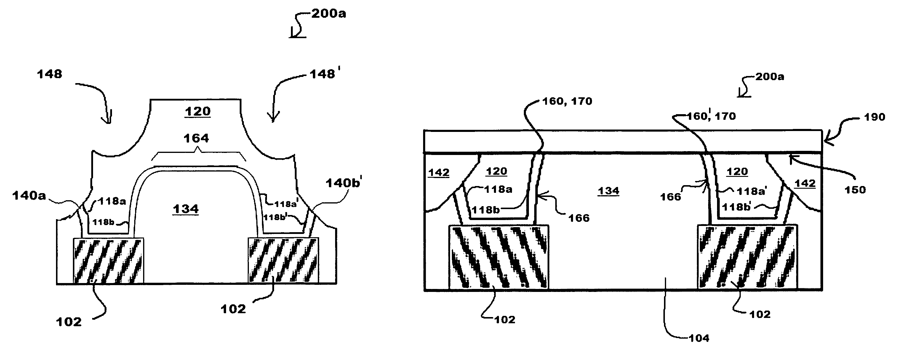
[0028]The invention relates to planarized segmented lower contacts that are flush with a planar surface adapted to receive a memory material such as a variable resistance memory material in a subsequent deposition step.

[0029]A method of the invention forms the planarized segmented lower contacts. The method first forms a lower electrode, deposits a first insulating layer thereon, uses a patterned wall mask...


PUM


Abstract

An electronic device including a planar segmented contact. A method for forming the device includes depositing a first insulator on a substrate, forming an opening in the first insulator, disposing a conductive material in the opening where the conductive material defines two or more conductive regions, forming a second insulator over the conductive layer, removing a portion of the second insulator to expose less than all of the conductive regions, recessing at least one of the exposed conductive regions, forming a third insulator over the recessed conductive region, and planarizing to expose at least one of the non-recessed conductive regions without exposing a recessed conductive region. An electrically stimulable material may then be formed over an exposed non-recessed conductive region.

Description

FIELD OF INVENTION[0001]This invention relates generally to programmable resistance and switching devices having one or more electrical contacts with a lithographic or sublithographic dimension. More particularly, this invention relates to programmable resistance and switching device structures with contacts formed from a planarized segmented ring contact using lithography and conventional deposition methods. Most particularly, this invention relates to programmable resistance and switching devices with sublithographic contacts having reduced structural irregularities, improved conformality, and reduced programming currents.BACKGROUND OF THE INVENTION[0002]The use of programmable variable resistance materials in electronic devices is known in the art. The chalcogenides are an important class of programmable variable resistance materials. The principles of operation of chalcogenide materials and devices are described in U.S. Pat. No. 5,296,716, No. 5,341,328, No. 5,359,205, and No. 7...

Claims


Application Information

Patent Timeline
Patent Type & Authority Patents(United States)
IPC IPC(8): H01L21/00
CPCH01L27/24H10B63/10H10B63/00
Inventor WICKER, GUY
Owner OVONYX MEMORY TECH LLC
Learn More