Method for forming an avalanche photodiode

a photodiode and avalanche technology, applied in the field of avalanche photodiodes, can solve the problems of reducing the breakdown voltage, increasing the dark count rate, and reducing the total so as to and reduce the volume of the device region.

Active Publication Date: 2009-06-30
LG INNOTEK CO LTD
View PDF17 Cites 0 Cited by
  • Summary
  • Abstract
  • Description
  • Claims
  • Application Information

AI Technical Summary

Benefits of technology

[0014]The present invention provides methods for fabricating an avalanche photodiode with separate absorption and multiplication layers (SAM-APD). In particular, the present invention provides methods for forming the multiplication layer of a SAM-APD. In some embodiments, APDs fabricated using the methods of the present invention provide high optical coupling efficiency and low dark count rate. Some APDs fabricated using methods of the present invention are particularly useful for single-photon detection applications. The present invention offers advantages over methods for APD fabrication, as they have been practiced in the prior art.
[0018]An aspect of the present invention is the inventors' recognition that the dark count rate is a function of the number of defects located in the device region of an APD, and that the dark count rate can be decreased by reducing the volume of the device region. In some embodiments, the total volume of the device region is reduced by decreasing the width of the edge region. The reduction in the volume of the device region is obtained without compromising a uniform gain profile or a uniform breakdown voltage profile across the device region.

Problems solved by technology

The curvature of the junction profile in the edge region, however, leads to a larger local electric field and therefore higher gain and lower breakdown voltage than in the active region.
Unfortunately, dark count rate also increases with overbias; therefore in many cases increased overbias actually degrades NEP rather than improves it.
Moreover, it is unlikely that defects will ever be completely eliminated through improved growth technique in a cost-effective manner.

Method used


Image

  • Method for forming an avalanche photodiode
  • Method for forming an avalanche photodiode
  • Method for forming an avalanche photodiode

Examples


Embodiment Construction

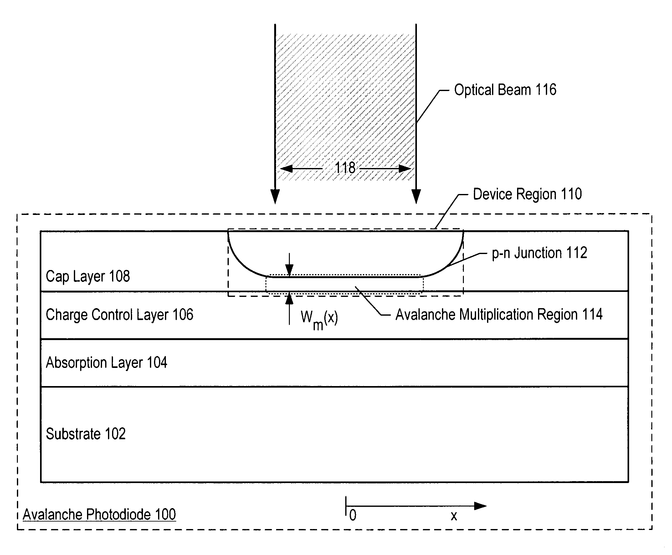
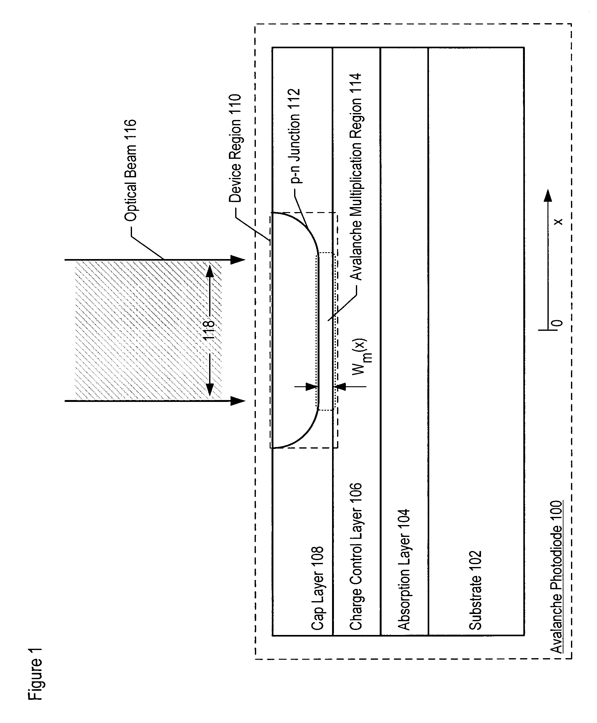
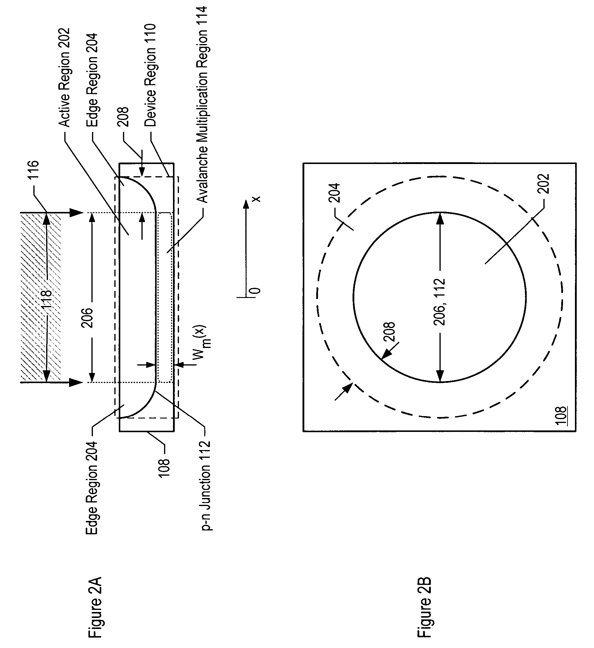
[0035]The following terms are defined for use in this Specification, including the appended claims:[0036]Device region is the portion of the cap layer defined by the lateral extent of the doped portion of the cap layer. The device region includes the full thickness of the cap layer, and therefore includes the undoped portion of the cap layer that resides under the doped portion. For example, the device region includes both the active region and the edge region, as defined below.[0037]Active region means that portion of the cap layer wherein the p-n junction has a substantially uniform doping profile and junction depth (i.e., wherein the p-n junction is a planar junction). The active region extends though the entire thickness of the cap layer, and therefore also includes the avalanche multiplication region under the planar junction.[0038]Edge region means that portion of the cap layer wherein the p-n junction does not have a substantially uniform doping profile and junction depth (i....


PUM


Abstract

Methods for fabricating an avalanche photodiode (APD), wherein the APD provides both high optical coupling efficiency and low dark count rate. The APD is formed such that it provides an active region of sufficient width to enable high optical coupling efficiency and a low dark count rate. Some APDs fabricated using these methods have a device area with an active region and an edge region, wherein the size of the active region is substantially matched to the mode-field diameter of an optical beam, and wherein the size of the edge region is substantially minimized and further wherein the device region maintains a substantially uniform gain and breakdown voltage.

Description

STATEMENT OF RELATED CASES[0001]This application is related to U.S. patent application Ser. No. 11 / 251,965, filed on even date herewith, and incorporated by reference herein.FIELD OF THE INVENTION[0002]The present invention relates to avalanche photodiodes in general and, more particularly, to avalanche photodiodes for use in single-photon detection applications.BACKGROUND OF THE INVENTION[0003]Avalanche photodiode (APD) structures that have separate absorption and multiplication layers (SAM-APDs) can provide electrical output signals with high fidelity (i.e., low noise). In a SAM-APD, the optical energy is absorbed and converted into electrical carriers in a layer specifically designed for efficient absorption (hereinafter, referred to as the “absorption layer”). The resulting electrical signal is amplified in a different layer specifically designed for efficient electrical carrier multiplication (hereinafter, referred to as the “cap layer”). By separating the absorption and multip...

Claims


Application Information

Patent Timeline
Patent Type & Authority Patents(United States)
IPC IPC(8): H01L21/20
CPCH01L31/1075
Inventor BEN-MICHAEL, RAFAELITZLER, MARK ALLEN
Owner LG INNOTEK CO LTD
Why Eureka
Try Eureka