Waveguide, waveguide module, optical transmission device, and method of manufacturing waveguide
a technology of waveguides and modules, applied in the field of waveguides, waveguide modules, optical transmission devices, and methods of manufacturing waveguides, can solve the problems of increased manufacturing costs, optical loss, and change in the amount of light that leaks out from the core to the clad, so as to prevent separation and enhance the reliability of optical properties
- Summary
- Abstract
- Description
- Claims
- Application Information
AI Technical Summary
Benefits of technology
Problems solved by technology
Method used
Image


Examples
embodiment 1
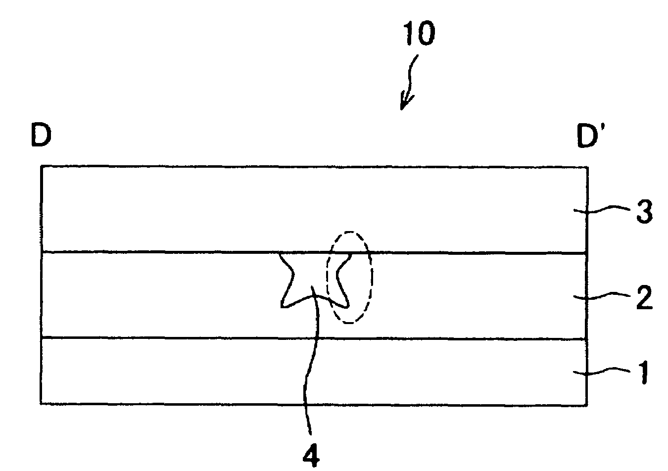
[0084]One embodiment of the present invention will now be described using the figures. FIG. 1(a) is a front view of a waveguide 10 according to the present embodiment, and FIG. 1(b) is a cross sectional view taken along the cross section of D-D′.
[0085]As shown in FIG. 1(b), the waveguide 10 is configured by a substrate 1, a lower clad (clad layer) 2, an upper clad (second clad layer) 3, and a core 4. The core 4 is formed so as to be surrounded by the groove (groove part) arranged in the lower clad 2, and is made of a material having a refraction index higher than the lower clad 2 and the upper clad 3. Thus, the light that has entered the core 4 from one end face of the core 4 is transmitted while being totally reflected at the interface of the clad 2, 3 and the core 4, and is exit from the other end face of the core 4.
[0086]The material of the substrate 1 is not particularly limited, but a glass substrate is used in the present embodiment.
[0087]The lower clad 2 is made of acrylic re...
embodiment 2
[0127]Other embodiments of the present invention will now be described. Same reference characters are denoted for the members having a similar function as in Embodiment 1 for the sake of convenience of explanation, and the description thereof will be omitted.
[0128]Similar to Embodiment 1, the waveguide according to the present embodiment includes a core 4 having a concave-convex part at least one part of the cross sectional shape, thereby obtaining the effects substantially the same as the waveguide 10 in Embodiment 1.
[0129]However, the present embodiment differs from Embodiments 1 and 2 in that the core 4 is formed using the semiconductor process.
[0130]A method of manufacturing the waveguide according to the present embodiment will now be described. FIGS. 3(a) and 3(b) are cross sectional views showing a part of the manufacturing steps of the waveguide according to the present embodiment.
[0131]First, an ultraviolet curable resin (clad material) is deposited on the substrate 1, and ...
embodiment 3
[0148]Other further embodiments of the present invention will now be described. Same reference characters are denoted for the members having a similar function as in Embodiment 1 for the sake of convenience of explanation, and the description thereof will be omitted.
[0149]With respect to the film waveguide (waveguide) 20 according to the present embodiment, the film waveguide (film waveguide) 20 having flexibility and having a total thickness of 300 μm is obtained by forming the upper and lower clad 2, 3 with thin thickness and removing the substrate (glass substrate) 1 in the waveguide 10 according to Embodiment 1. That is, the film waveguide 20 is configured by a stacked body of resin layers having a total thickness of 300 μm and flexibility so as to be used in a bent manner, used winded around the shaft etc., arranged so as to be allowed to be twisted etc.
[0150]In the film waveguide 20, the acceptable amount with respect to the shearing force by stretching property increases etc....
PUM
| Property | Measurement | Unit |
|---|---|---|
| flexural modulus | aaaaa | aaaaa |
| total thickness | aaaaa | aaaaa |
| elastic modulus | aaaaa | aaaaa |
Abstract
Description
Claims
Application Information
 - R&D
- Intellectual Property
- Life Sciences
- Materials
- Tech Scout
- Unparalleled Data Quality
- Higher Quality Content
- 60% Fewer Hallucinations
Browse by: Latest US Patents, China's latest patents, Technical Efficacy Thesaurus, Application Domain, Technology Topic, Popular Technical Reports.
© 2025 PatSnap. All rights reserved.Legal|Privacy policy|Modern Slavery Act Transparency Statement|Sitemap|About US| Contact US: help@patsnap.com