
Method for manufacturing a wiring over a substrate

a manufacturing method and technology for wiring, applied in the direction of printed circuit manufacturing, optics, instruments, etc., can solve the problems of deterioration of the insulating layer provided between the wiring, short circuiting or short circuiting of the wiring, and increase the projection and depression difference, so as to prevent short circuiting between the wiring and the insulating layer from cracking, the effect of high yield

Inactive Publication Date: 2009-05-26
SEMICON ENERGY LAB CO LTD
View PDF22 Cites 4 Cited by
  • Summary
  • Abstract
  • Description
  • Claims
  • Application Information

AI Technical Summary

Benefits of technology

The present invention provides a method for manufacturing a wiring over a substrate that can reduce particles between wirings, prevent short-circuiting between wirings, and prevent cracking in the insulating layer. The method involves forming a first conductive layer over an insulating surface, making a first mask pattern over the first conductive layer, etching the first conductive layer under a first condition to form a second conductive layer, and etching the second conductive layer under a second condition to form a third conductive layer. The method can produce a wiring with high yield and reliability.

Problems solved by technology

However, there is a problem of disconnection or short-circuiting of the wiring due to particles such as contaminant particles since the space between the wirings becomes narrowed due to the increase of the number of wirings.
In the semiconductor device having a multi-wire structure, the width of the wiring is miniaturized and the density of the wiring is increased, which leads that a difference in projection and depression is increased and the coverage of an insulating layer provided between wirings is deteriorated.
Therefore, there is another problem that a lower wiring and an upper wiring are short-circuited.
As a result, cracks are produced in the insulating layer, which results in another problem.
The cracks in the insulating layer yields problems that irregularities are produced over the surface of the insulating layer; corrosion of the lower wiring due to penetration of moisture from the crack; and short-circuiting of the upper wiring and the lower wiring at the crack.
Further, particles remained between wirings also cause cracks and irregularities over the surface of the insulating layer.
In the case of forming a light-emitting element over the insulating layer, an anode and a cathode of the light-emitting element are short-circuited, which leads to the deterioration of the light-emitting element.
When a crack is occurred in a certain portion of the insulating layer, cracks become readily occurred in another regions.
That is, cracks become into a chain reaction.

Method used


Image

  • Method for manufacturing a wiring over a substrate
  • Method for manufacturing a wiring over a substrate
  • Method for manufacturing a wiring over a substrate

Examples


embodiment 1

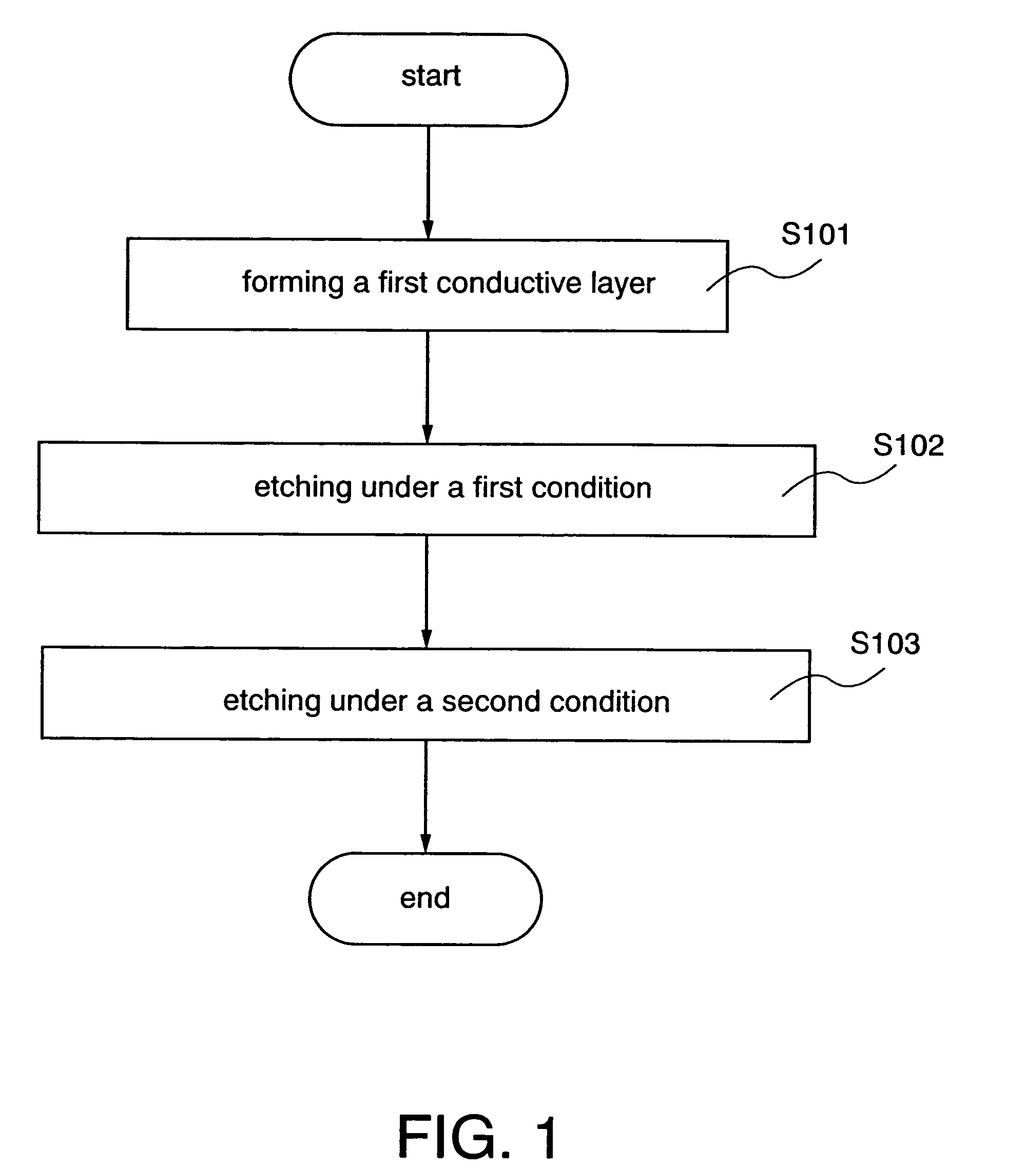
[0049]In this embodiment, a method for manufacturing a wiring over a substrate comprising a wiring having a side with a curved face by an etching process under a first condition and an etching process under a second condition is explained with reference to FIGS. 1, 3A to 3D, and 7.

[0050]As illustrated in FIG. 3A, a first insulating layer 101 is formed over a substrate 100, and a first conductive layer 102 is formed over the first insulating layer 101. Then, a first mask pattern 103 is formed over the first conductive layer 102 (a step S101 in FIG. 1).

[0051]As the substrate 100, a substrate made from an insulating material such as a glass substrate, a quartz substrate, or alumina substrate; a plastic substrate having heat resistance that can resist processing temperature in a later process; a silicon wafer; a metal plate; or the like can be used. In this instance, an insulating film for preventing dispersion of impurities from the substrate such as silicon oxide (SiOx), silicon nitri...

embodiment 2

[0069]In this embodiment, a method for manufacturing a wiring having a side with a curved face according to a different etching condition from that explained in Embodiment 1 is explained with reference to FIGS. 1, 4A to 4D, and 7.

[0070]As illustrated in FIG. 4A, as is the case with Embodiment 1, a first insulating layer 101 is formed over a substrate 100, and a first conductive layer 102 is formed over the first insulating layer 101. Then, a first mask pattern 103 is formed over the first conductive layer 102 (a step S101 in FIG. 1).

[0071]As illustrated in FIG. 4B, the first conductive layer 102 is etched by using the first mask pattern 103 under a first condition to form a second conductive layer 211 having a side perpendicular to the first mask pattern 103 (a step S102 in FIG. 1). The first condition is the condition by which the first conductive layer 102 is anisotropically etched, typically, a conductive layer having a perpendicular side is formed. Further typically, the first c...

embodiment 3

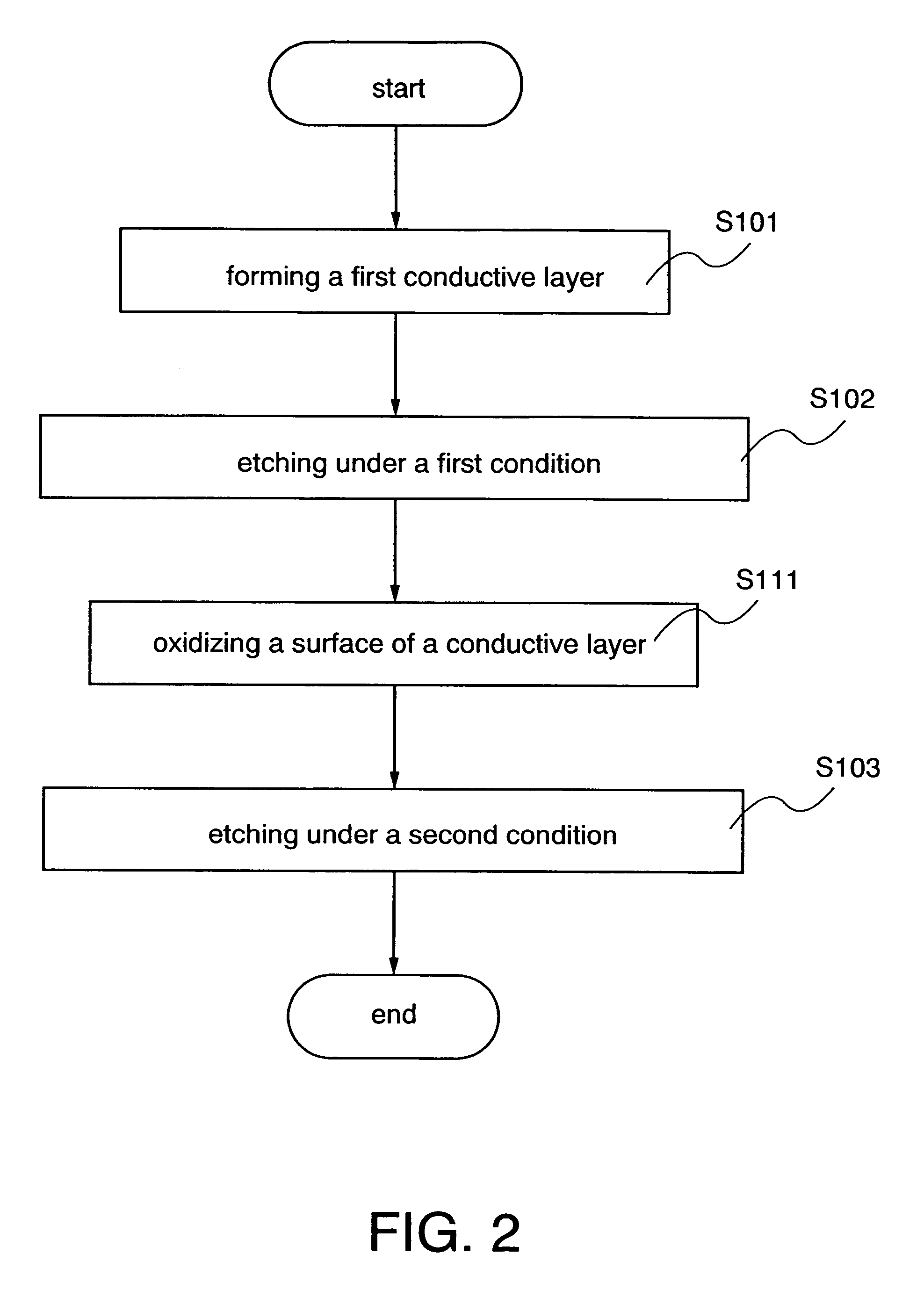
[0078]In this embodiment, a method for manufacturing a wiring having a side having a plurality of inclined planes according to a different etching process from that in Embodiments 1 and 2 is explained with reference to FIGS. 2, 5A to 5F, and 8.

[0079]As illustrated in FIG. 5A, a first insulating layer 101 is formed over a substrate 100 as is the case with Embodiment 1, and a first conductive layer 102 is formed over the first insulating layer 101. Then, a first mask pattern 103 is formed over the first conductive layer 102 (a step S101 in FIG. 2).

[0080]As illustrated in FIG. 5B, the first conductive layer 102 is etched by using the first mask pattern 103 under a first condition to form a second conductive layer 302 (a step S102 in FIG. 2). The first condition is the condition by which the first conductive layer 102 is etched, therefore, a conductive layer having a tapered edge is formed. In this instance, the first condition in this example is the same as that in Embodiment 1. Note t...


PUM

PropertyMeasurementUnit
angleaaaaaaaaaa
angle of inclinationaaaaaaaaaa
angleaaaaaaaaaa

Abstract

A wiring over a substrate capable of reducing particles between wirings and a method for manufacturing the wiring is disclosed. A wiring over a substrate capable of preventing short-circuiting between wirings due to big difference in projection and depression between wirings and a method for manufacturing the wiring is also disclosed. Further, a wiring over a substrate capable of preventing cracks in the insulating layer due to stress at the edge of a wiring or particles and a method for manufacturing the wiring is also disclosed. According to the present invention, a method for manufacturing a wiring over a substrate is provided that comprises the steps of: forming a first conductive layer over an insulating surface; forming a first mask pattern over the first conductive layer; forming a second mask pattern by etching the first mask pattern under a first condition, simultaneously, forming a second conductive layer having a side having an angle of inclination cross-sectionally by etching the first conductive layer; and forming a third conductive layer and a third mask pattern by etching the second conductive layer and the second mask pattern under a second condition; wherein a selective ratio under the first condition of the first conductive layer to the first mask pattern is in a range of 0.25 to 4, and a selective ratio under the second condition of the second conductive layer to the second mask pattern is larger than that under the first condition.

Description

BACKGROUND OF THE INVENTION[0001]1. Field of the Invention[0002]The present invention relates to a method for manufacturing a wiring over a substrate and a semiconductor device having a multi-wire structure.[0003]2. Related Art[0004]In recent years, a wiring over a substrate and a semiconductor device are highly integrated since the degree of integration of a semiconductor element is improved. Accordingly, the width of a wiring is further miniaturized, and the number of wirings is increased. Moreover, an area of the semiconductor device is reduced by being the wiring into multi-wire.[0005]However, there is a problem of disconnection or short-circuiting of the wiring due to particles such as contaminant particles since the space between the wirings becomes narrowed due to the increase of the number of wirings.[0006]In the semiconductor device having a multi-wire structure, the width of the wiring is miniaturized and the density of the wiring is increased, which leads that a differenc...

Claims


Application Information

Patent Timeline
Patent Type & Authority Patents(United States)
IPC IPC(8): H01L21/302G02F1/1362H01L21/3213H01L21/461H01L21/4763H01L21/768H01L27/32
CPCH01L21/32136H01L21/32137H01L21/32139H01L27/3276H01L51/0021H05K3/06G02F2001/13629H01L2924/0002H01L51/0023H01L51/5281H05K2203/0315H05K2203/0346H05K2203/095H05K2203/1476H01L2924/00G02F1/13629H10K59/131H10K71/60H10K71/621H10K59/8791H01L27/124H10K50/86
Inventor SASAGAWA, SHINYAOKAMOTO, SATORUMONOE, SHIGEHARU
Owner SEMICON ENERGY LAB CO LTD
Learn More