Dry etching method and diffractive optical element
a technology of diffractive optical elements and dry etching methods, which is applied in the direction of optical elements, thermoelectric devices, instruments, etc., can solve the problems of complex structure of dry etching apparatus, achieve stable etching rate, suppress the increase in the temperature of insulative substrates, and reduce the effect of temperature increas
- Summary
- Abstract
- Description
- Claims
- Application Information
AI Technical Summary
Benefits of technology
Problems solved by technology
Method used
Image

Examples
example 2
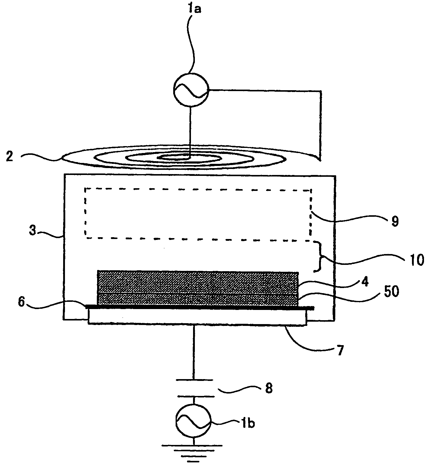
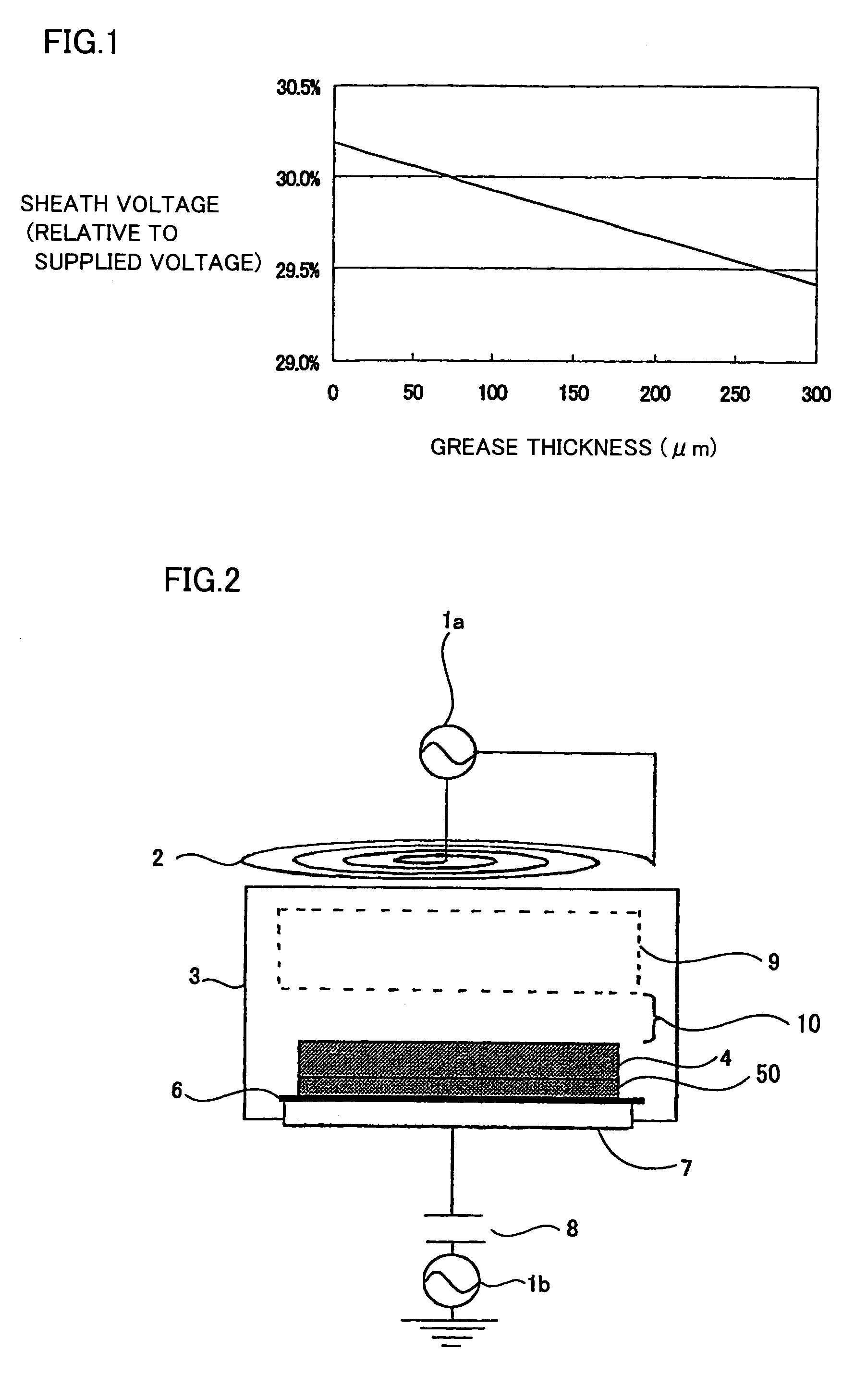
[0050]As shown in FIG. 5A, three insulative substrates 4 (A to C) composed of synthetic fused silica were placed on conductor 6 implemented by the conductive Si wafer shown in FIG. 2. Here, as shown in FIG. 5B, three insulative substrates 4 were placed on conductor 6 with conductive grease 50 obtained by blending carbon in silicon oil (resistivity: 49Ω·cm, “KS660” manufactured by Shin-etsu Silicone) being interposed. Each of three insulative substrates 4 (A to C) had a diameter of 50 mm and a thickness of 5 mm.
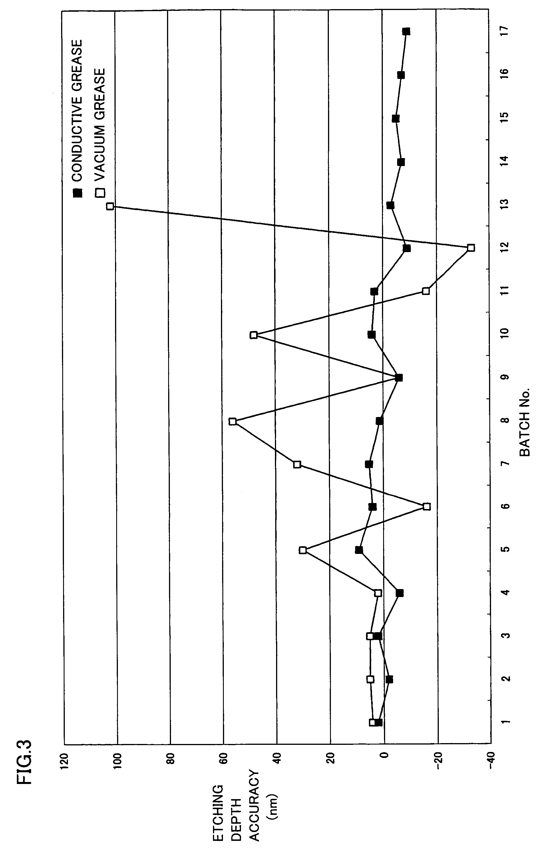
[0051]Thereafter, insulative substrates 4 (A to C) were subjected to dry etching, as in Example 1. Then, the depth of the etched groove in each of insulative substrates 4 (A to C) after dry etching was measured. Table 1shows the depth of the etched groove measured in Example 2.
[0052]In Example 2, dry etching was performed such that the depth of the etched groove in each of three insulative substrates 4 (A to C) was set to 1200 nm. In addition, both of dry etching and measureme...
example 3
[0057]As shown in FIG. 6A, 19 insulative substrates 4 (A to S) composed of synthetic fused silica were placed on conductor 6 implemented by the conductive Si wafer shown in FIG. 2. Here, as shown in FIG. 6B, 19 insulative substrates 4 (A to S) were placed on conductor 6 with conductive grease 50 obtained by blending carbon in silicon oil (resistivity: 49Ω·cm, “KS660” manufactured by Shin-etsu Silicone) being interposed. Each of 19 insulative substrates 4 (A to S) had a diameter of 20 mm and a thickness of 3 mm.
[0058]Thereafter, insulative substrates 4 (A to S) were subjected to dry etching, as in Example 1. Then, the depth of the etched groove in each of insulative substrates 4 (A to S) after dry etching was measured. Table 2 shows the depth of the etched groove measured in Example 3.
[0059]In Example 3, dry etching was performed such that the depth of the etched groove in each of 19 insulative substrates 4 (A to S) was set to 1200 nm. In addition, both of dry etching and measurement...
example 4
[0064]As shown in FIG. 7A, four insulative substrates 4 (A to D) composed of ZnSe polycrystal were placed on conductor 6 implemented by the conductive Si wafer shown in FIG. 2. Here, as shown in FIG. 7B, four insulative substrates 4 (A to D) were placed on conductor 6 with conductive grease 50 obtained by blending carbon in silicon oil (resistivity: 49Ω·cm, “KS660” manufactured by Shin-etsu Silicone) being interposed. Each of four insulative substrates 4 (A to D) had a diameter of 50 mm and a thickness of 5 mm.
[0065]Then, chamber 3 was evacuated until the pressure therein was set to approximately 10−5 Pa, and BCl3 (flow rate: 10 sccm) and Ar (flow rate: 20 sccm) were introduced into chamber 3. In succession, while the pressure within chamber 3 was set to 3 Pa, four insulative substrates 4 (A to D) were dry-etched by plasma 9 generated as a result of application of high-frequency power to RF power supplies 1a, 1b (ICP power: 200 W, RF power: 300 W). Then, the depth of the etched groo...
PUM
 Abstract
Description
Claims
Application Information
 - R&D
- Intellectual Property
- Life Sciences
- Materials
- Tech Scout
- Unparalleled Data Quality
- Higher Quality Content
- 60% Fewer Hallucinations
Browse by: Latest US Patents, China's latest patents, Technical Efficacy Thesaurus, Application Domain, Technology Topic, Popular Technical Reports.
© 2025 PatSnap. All rights reserved.Legal|Privacy policy|Modern Slavery Act Transparency Statement|Sitemap|About US| Contact US: help@patsnap.com