Sustaining circuit with bi-directional device

a bi-directional device and support circuit technology, applied in the direction of semiconductor devices, semiconductor/solid-state device details, instruments, etc., can solve the problems of large capacity required, reduced circuit size and loss, and limitation in view of energy consumption resulting from circuit size reduction, etc., to achieve effective suppression of the increase in the temperature of inventive devices, excellent heat dissipation properties, and small loss

Inactive Publication Date: 2009-04-21
PANASONIC CORP
View PDF5 Cites 8 Cited by
  • Summary
  • Abstract
  • Description
  • Claims
  • Application Information

AI Technical Summary

Benefits of technology

[0009]It is therefore an object of the present invention to provide a switching device with a reduced area size and suppressed power loss.
[0011]With this structure, for example, if each of the first and second transistors is a transistor in which a current flows in the vertical direction, a switching operation can be performed even though the polarity of a voltage applied between the second and fourth electrodes is changed. Thus, the semiconductor device can be driven by an alternating current. Moreover, two transistors are stacked, so that a circuit area can be reduced to about ½, compared to the case where two transistors are arranged side by side on the same substrate. Furthermore, the substrate formed of a wide bandgap semiconductor is used, so that a current density can be increased, compared to the case where a known Si substrate is used. Thus, a device size can be largely reduced.
[0013]If each of the first transistor and the second transistor is a vertical-type MISFET, each of the first electrode and the third electrode is a source electrode, each of the second electrode and the fourth electrode is a drain electrode, and each of the first control electrode and the second control electrode is a gate electrode, a bi-directional device with small loss can be achieved.
[0014]If each of the first substrate and the second substrate is formed of silicon carbide, increase in the temperature of the inventive device can be effectively suppressed, compared to the case where a silicon substrate is used, because silicon carbide has excellent heat dissipation properties. Moreover, the current density of silicon carbide is about 10 times larger than that of silicon. Thus, with a current at the same level, a planar size of the semiconductor device of the present invention can be reduced to about 1 / 10 of a known semiconductor device in which two transistors are stacked. Accordingly, the size of the semiconductor device of the present invention can be reduced to about 1 / 20 of that of a known semiconductor device in which tow transistors are arranged in the lateral direction. Moreover, a relatively small semiconductor can be fabricated in a simple manner, compared to the case where some other wide bandgap semiconductor is used.
[0016]If the inventive semiconductor device further includes: a first metal plate adhered to the back surface of the first substrate; and a second metal plate adhered to the back surface of the second substrate, packaging can be performed to a circuit substrate in a simple manner and, furthermore, heat dissipation properties can be improved.
[0018]With this structure, the area of the sustaining circuit can be reduced and simplified, compared to the case where a large number of known transistors formed of Si are arranged. Moreover, since a wide bandgap semiconductor has low loss and excellent heat resistance, an equipment for cooling the device can be omitted. As a result of use of the sustaining circuit of the present invention, the structure of a driver circuit for a PDP can be simplified.

Problems solved by technology

However, when AC-DC conversion is performed by the AC-DC conversion circuit, a current flows in the diode, thus resulting in conduction loss.
Furthermore, a large capacity is required if a large capacity capacitor is provided.
Therefore, for the known switching device, there is a limitation in view of energy consumption resulting from reduction in a circuit size and loss.

Method used


Image

  • Sustaining circuit with bi-directional device
  • Sustaining circuit with bi-directional device
  • Sustaining circuit with bi-directional device

Examples


first embodiment

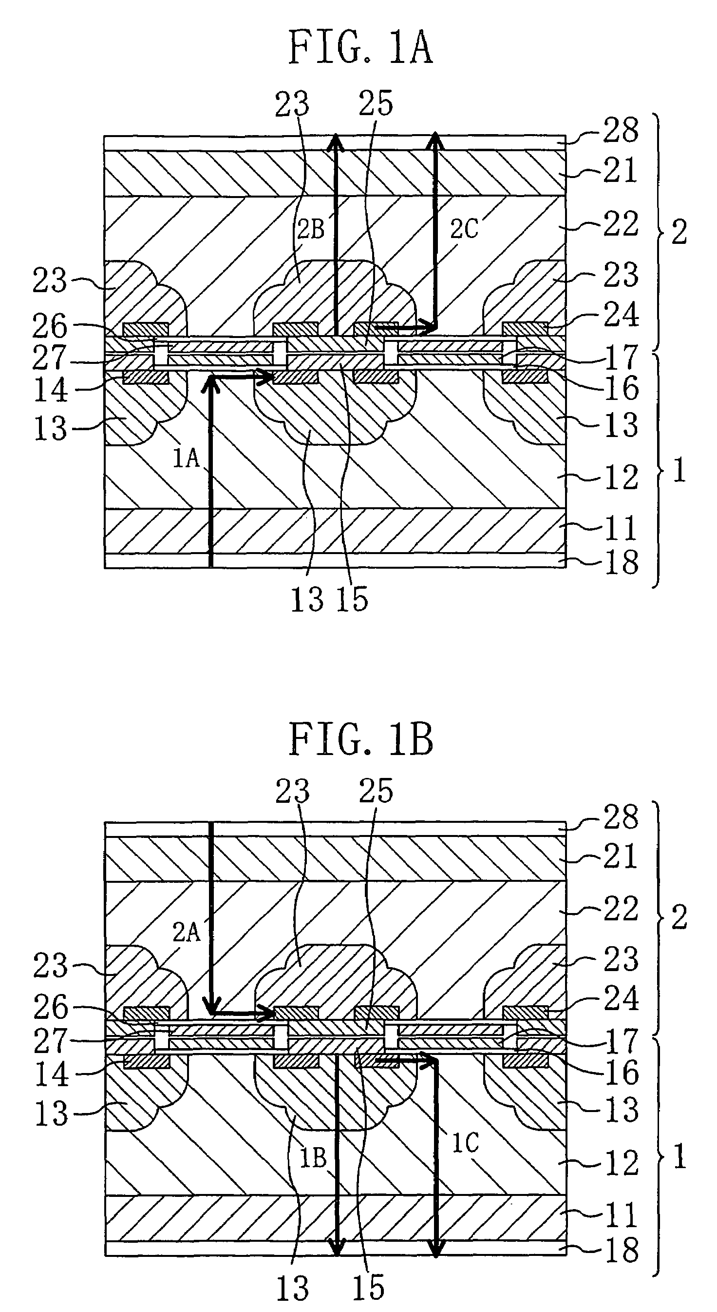
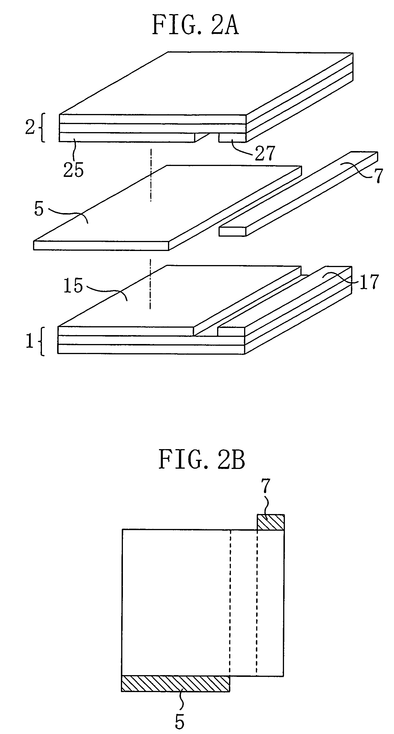
[0036]FIGS. 1A and 1B are cross-sectional views illustrating bi-directional device according to a first embodiment of the present invention.

[0037]As shown in FIGS. 1A and 1B, the bi-directional device of the present invention includes a first switching device 1, a second switching device 2 formed on the first switching device 1 so that a principal surface side thereof faces a principal surface side of the second switching device 2. In this example, the first and second switching devices 1 and 2 are vertical-type MOSFETs each having the same electric properties. Note that in this application, a principal surface side of a switching device corresponds to a principal surface side of a substrate.

[0038]As shown in FIGS. 1A and 1B, the first switching device 1 includes a substrate 11 formed of an n-type SiC, an n-type doped layer (drain layer) 12 epitaxially grown over the principal surface of the substrate 11, formed of nitrogen-containing SiC, and having a thickness of 10 μm, a p-type w...

second embodiment

[0067]As a second embodiment of the present invention, a sustaining circuit using the bi-directional device described in the first embodiment will be described. The sustaining circuit is part of a driver circuit for a PDP.

[0068]FIG. 4 is a circuit diagram of a sustaining circuit according to the second embodiment. FIG. 5 is a waveform chart illustrating the waveform of an output current and the waveform of an output voltage of the sustaining circuit of FIG. 4.

[0069]The sustaining circuit of the PDP is a driver circuit for supplying a sustaining pulse voltage to an electrode of the PDP to emit light for display. As shown in FIG. 5, the sustaining circuit of this embodiment includes an output section for outputting a driving voltage of the PDP, first and second switching devices 82 and 83 each of which is an n-channel vertical-type MOSFET, an inductance 84, a capacitor 85, a third switching device 81 which is an n-channel vertical-type MOSFET, a fourth switching device 80, a first gat...


PUM


Abstract

At least two switching devices each including a substrate formed of a wide bandgap semiconductor, source and gate electrodes formed in a principal surface side of the substrate, and a drain electrode formed on the back surface of the substrate are stacked so that respective upper surface sides of the switching face each other.

Description

RELATED APPLICATION[0001]This application is a divisional of U.S. application Ser. No. 10 / 736,672, filed Dec. 17, 2003, now U.S. Pat. No. 6,995,473, which in turn claims the benefit of Japanese Patent Application No. 2002-367848, filed Dec. 19, 2002, the disclosures of which Applications are incorporated by reference herein.BACKGROUND OF THE INVENTION[0002]The present invention relates to semiconductor power device, and more particularly relates to a semiconductor device which is formed of a wide bandgap semiconductor and in which a bi-directional switching operation can be performed and a sustaining circuit using the semiconductor device.[0003]Semiconductor power devices are used in power electronic applications in which high voltage is applied and used for high current power switches of electronic instruments.[0004]A known semiconductor power device such as a diode, a vertical-type MOSFET or the like has a pn juction. In this structure, current does not flow due to a depletion lay...

Claims


Application Information

Patent Timeline
Patent Type & Authority Patents(United States)
IPC IPC(8): H01L23/14H01L29/78H01L25/065H01L25/18H01L27/06
CPCH01L25/074H01L27/0694G09G3/294G09G3/2965H01L2924/1305H01L2924/1301H01L2924/01019H01L2224/48247H01L2224/48091G09G2330/028H01L2224/48137H01L2924/01079H01L2924/13055H01L2924/13091H01L2924/19041H01L2924/30107H01L2924/00014H01L2924/00H01L2224/0603H01L29/78
Inventor KITABATAKE, MAKOTOASADA, KAZUHIKOYAMASHITA, HIDEKAZUNAGAGATA, NOBUYOSHINOBORI, KAZUHIROOMORI, HIDEKIOGAWA, MASANORI
Owner PANASONIC CORP
Why Eureka
Try Eureka