
Surface mounting semiconductor device

a semiconductor and surface mounting technology, applied in the direction of solid-state devices, basic electric elements, electric apparatus construction details, etc., can solve the problems of poor reliability of solder joints, large influence on the efficiency reduction of light emission, poor state, etc., to achieve reliable mounting on circuit boards, good mounting properties, stable state

Inactive Publication Date: 2009-03-03
STANLEY ELECTRIC CO LTD
View PDF13 Cites 48 Cited by
  • Summary
  • Abstract
  • Description
  • Claims
  • Application Information

AI Technical Summary

Benefits of technology

[0020]The presently disclosed subject matter has been made in consideration of the above and other problems and accordingly can result in a product that has the ability to provide a surface mounting semiconductor device having nice mounting properties with good mounting reproducibility, excellent resistance to different environments, good thermal radiation properties, optical properties and electrical properties, high reliability, and other advantages.
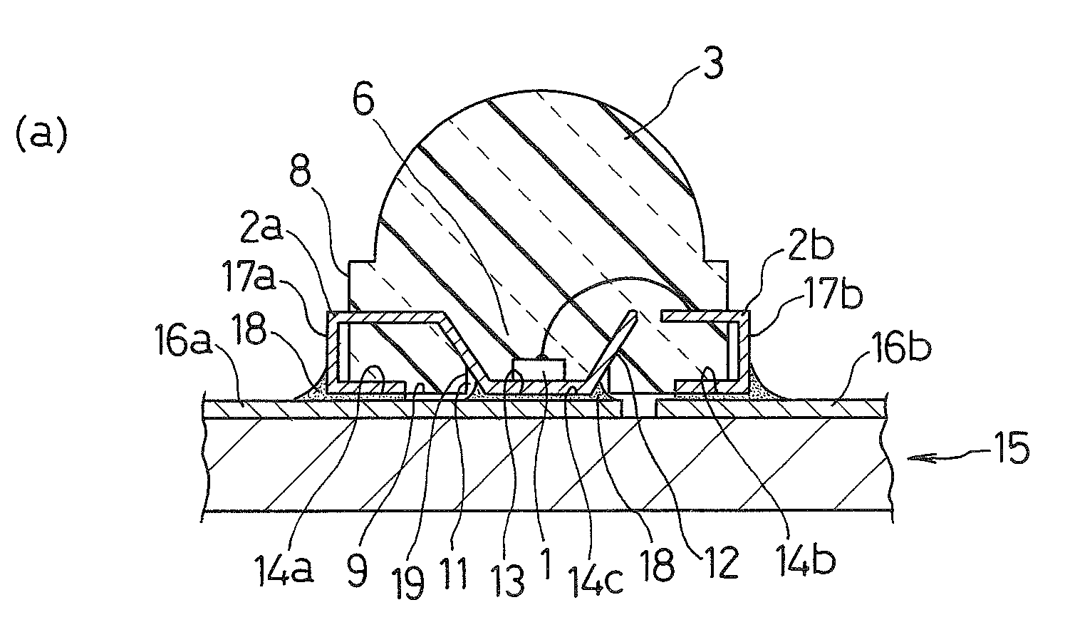
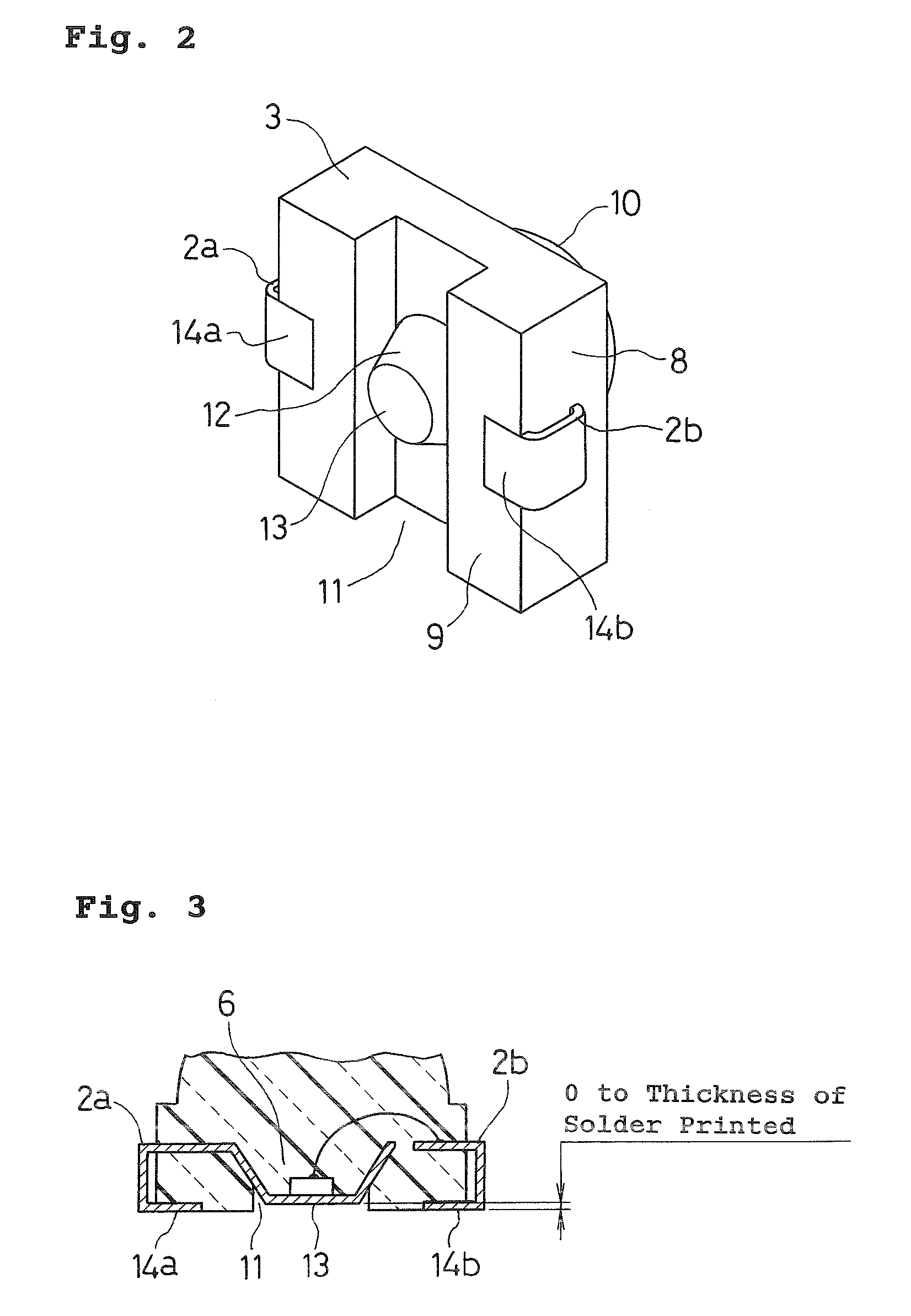
[0027]Therefore, the surface mounting semiconductor device can be mounted on the circuit board reliably and in a stable state. In addition, the conductor pattern on the circuit board located immediately beneath the semiconductor element can be connected electrically and / or thermally through a short path. As a result, it is possible to realize a surface mounting semiconductor device having nice mounting properties, including good mounting reproducibility, excellent resistance to different environments, good thermal radiation properties, optical properties and / or electrical properties, and / or high reliability.

Problems solved by technology

Therefore, the conditions of formation of the solder joints are not made uniform as described above, and accordingly the LED device is mounted in a poor state and made unstable, with poor reliability on the solder joint.
Particularly, in an LED device of the type that requires a large current to drive the LED chip 51, a failure to achieve excellent thermal radiation results in a large influence on reducing the efficiency of light emission.
The reproducibility of the tilt of the mounted LED device toward the circuit board 56 is poor with regard to the tilted angle α, resulting in worsened optical characteristics such as variations in distribution characteristic of the LED light.
Accordingly, the solder joints may be brought into contact with each other to cause electrical malfunctions.
Thus, it may be impossible to eliminate occurrences of failed products within the production processes.

Method used


Image

  • Surface mounting semiconductor device
  • Surface mounting semiconductor device
  • Surface mounting semiconductor device

Examples


Embodiment Construction

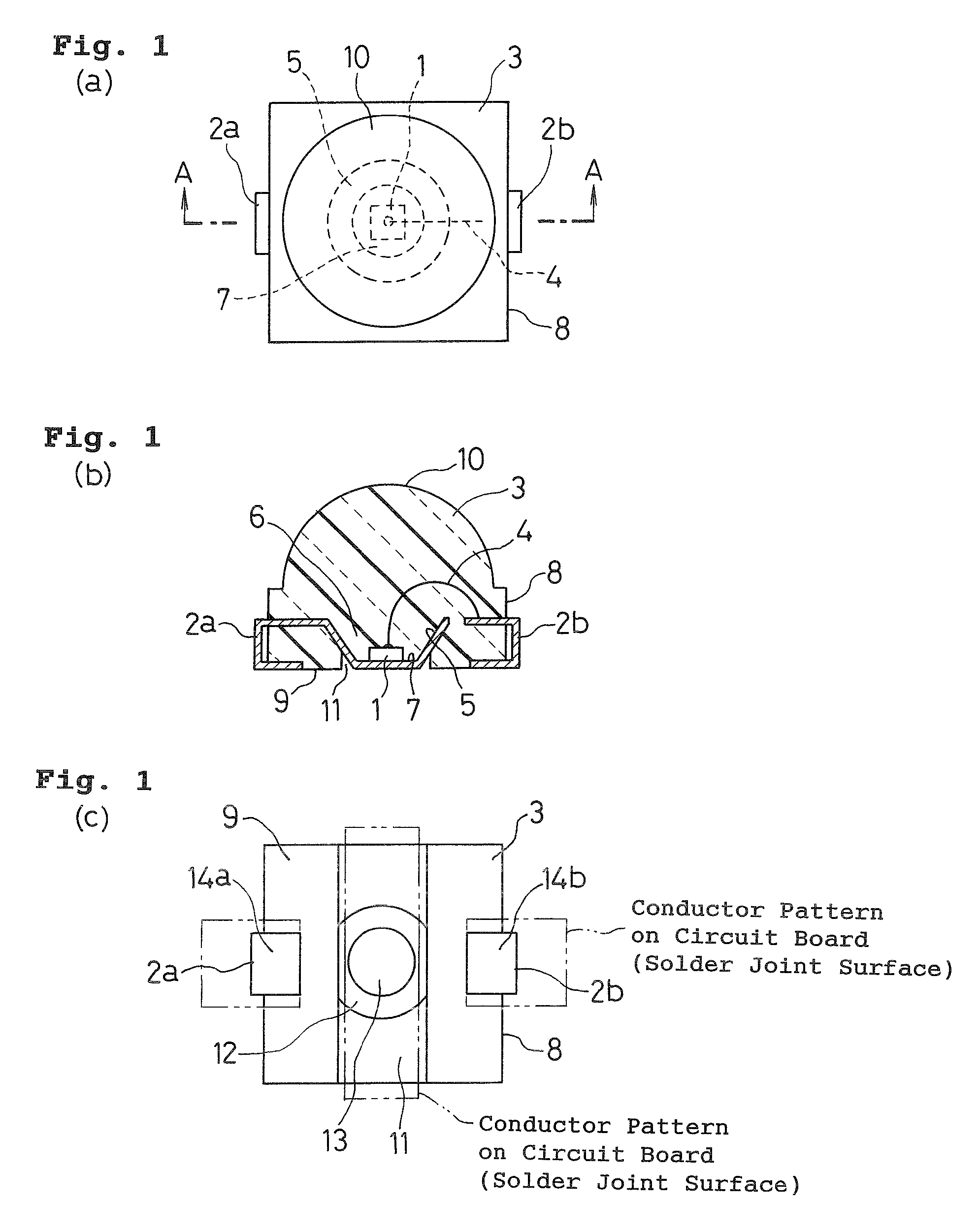
[0041]A surface mounting semiconductor device having nice mounting properties with good mounting reproducibility, excellent resistance to different environments, good thermal radiation properties, optical properties and electrical properties, high reliability, and / or other advantageous features is possible according to the disclosed subject matter herein. A semiconductor element can be mounted on an inner bottom surface of a recess formed in a lead frame and sealed in a resin. An outer bottom surface and an outer circumferential surface of the recess can be at least partly externally exposed from the sealing resin. The exposed portion(s) of the recess can be bonded to conductor patterns on a circuit board via a bonding agent having electrical conduction and / or thermal conduction. Such mounting can be adopted to achieve the above-noted features of the disclosed subject matter.

[0042]Exemplary embodiments of the disclosed subject matter will now be described in detail with reference to...


PUM


Abstract

In accordance with one example of the disclosed subject matter, a semiconductor device can include the following features. A first lead frame can be provided that has one end configured to form a recess. An LED chip can be mounted on an inner bottom surface of the recess. A bonding wire has one end connected to an electrode on the LED chip. A second lead frame has one end connected to the other end of the bonding wire. The LED chip and the bonding wire can be sealed in a sealing resin. The first lead frame and the second lead frame can protrude from the sealing resin and can be bent around to the bottom of the sealing resin. A groove formed through the center of the bottom of the sealing resin at least partly exposes an outer circumferential surface and an outer bottom surface of the recess from the sealing resin and into the groove.

Description

[0001]This application claims the priority benefit under 35 U.S.C. §119 of Japanese Patent Application No. 2005-221154 filed on Jul. 29, 2005, which is hereby incorporated in its entirety by reference.BACKGROUND[0002]1. Field[0003]The disclosed subject matter of the present application relates to a surface mounting semiconductor device, and more particularly to a surface mounting semiconductor device that can be equipped with a semiconductor element such as an IC, a diode, a light-emitting diode (LED), a photodiode, a PIN diode, a phototransistor, and / or other similar semiconductor components.[0004]2. Description of the Related Art[0005]Surface mounting semiconductor devices with various structures have been previously proposed. One conventional art example is structured as shown in FIG. 12 and includes lead frames 50a, 50b, 50c that are separated and arranged at three locations. On the first lead frame 50a, a semiconductor element (such as an LED chip 51) is mounted, with a thermal...

Claims


Application Information

Patent Timeline
Patent Type & Authority Patents(United States)
IPC IPC(8): H05K7/10H01L33/54H01L33/56H01L33/60H01L33/62H01L33/64
CPCH01L33/486H01L33/62H01L33/60H01L2224/48091H01L2224/48247H01L2224/48465H01L2924/01078H01L2924/00014H01L2924/00H01L2924/1815
Inventor TANAKA, KOZOSEKI, SHINICHI
Owner STANLEY ELECTRIC CO LTD
Learn More