
MOSFETs comprising source/drain regions with slanted upper surfaces, and method for fabricating the same

a technology of mosfets and source/drain regions, which is applied in the field of metaloxidesemiconductor field effect transistors, can solve the problems of reducing the overall contact resistance of mosfets, compressive or tensile stress may be generated in the channel region of mosfets, etc., and achieves improved stress profile, enhanced stress strength, and higher carrier mobility

Inactive Publication Date: 2009-02-03
IBM CORP +1
View PDF14 Cites 17 Cited by
  • Summary
  • Abstract
  • Description
  • Claims
  • Application Information

AI Technical Summary

Benefits of technology

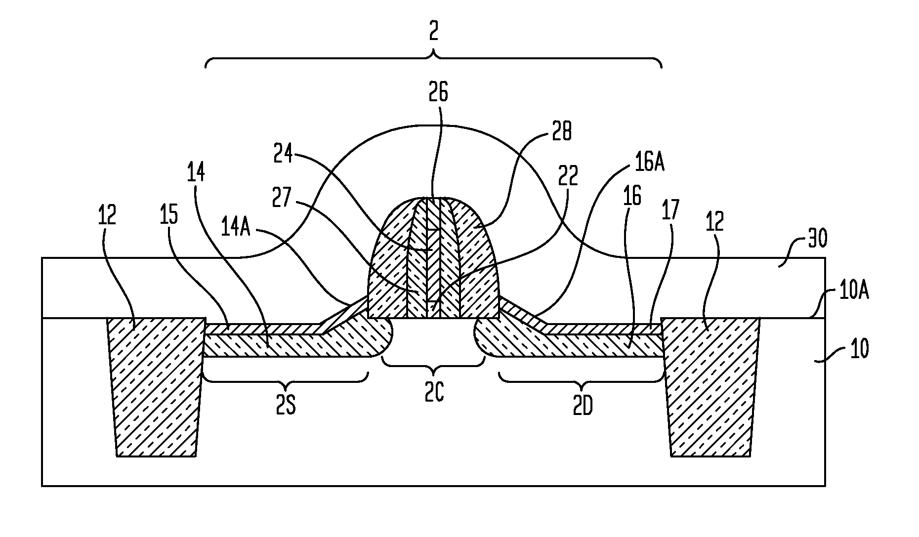
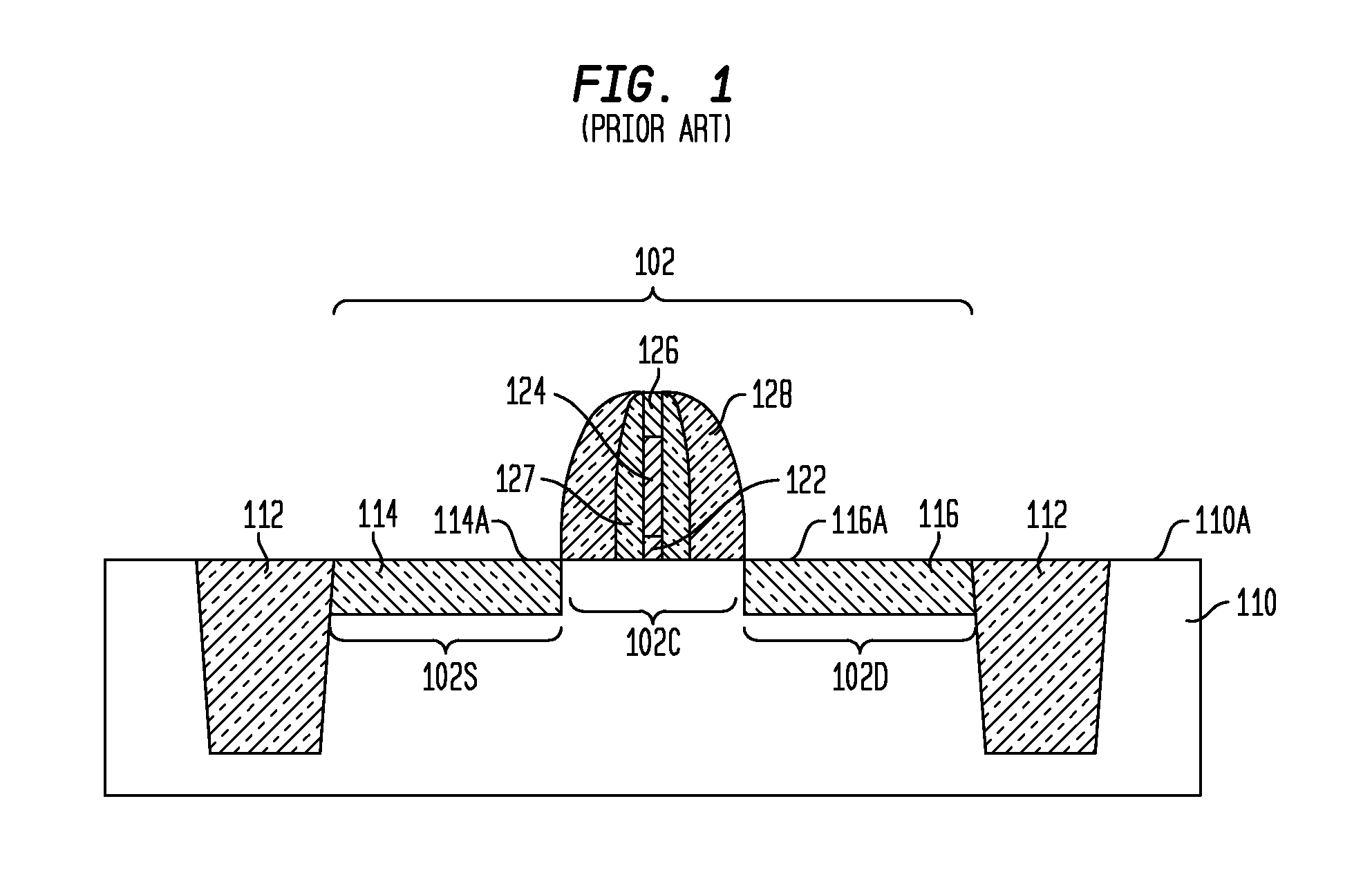
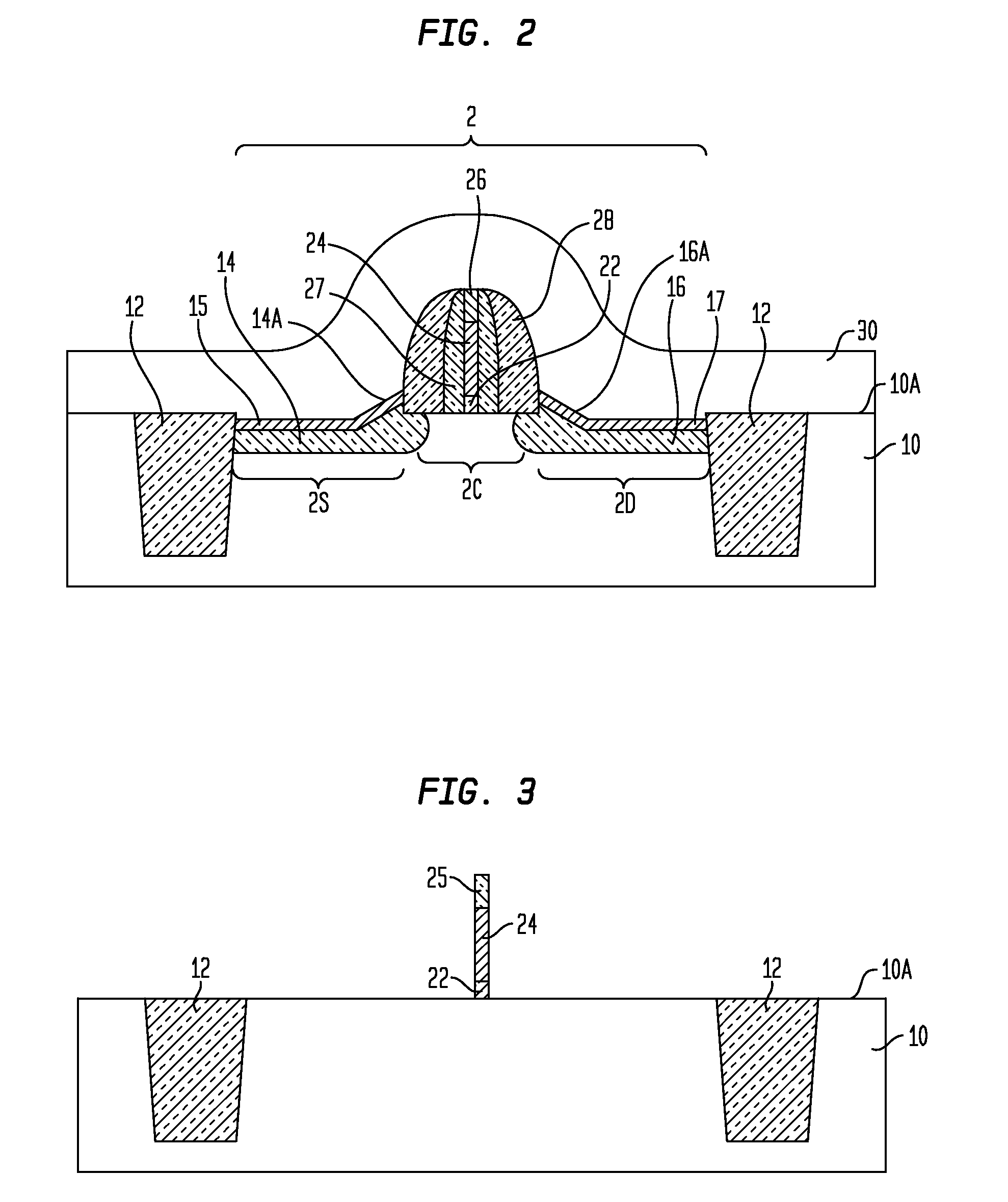
The present invention relates to a semiconductor device comprising a MOSFET with slanted source and drain regions. By recessing the source and drain regions before epitaxially growing materials to refill them, a properly tailored recess profile can be created that results in slanted upper surfaces. These slanted surfaces enhance the strength of stress and establish better stress profile in the channel region of the MOSFET, leading to higher carrier mobility and better contact area and reduced contact resistance. The method for forming the semiconductor device involves crystallographically etching the substrate to form surface recesses, growing semiconductor material in the recesses to form semiconductor structures with slanted upper surfaces, and optionally adding a stress-inducing dielectric capping layer.

Problems solved by technology

Further, such source and drain regions with slanted upper surfaces can increase the contact area and reduce the overall contact resistance of the MOSFETs.
In this manner, compressive or tensile stress may be generated in the channel region of the MOSFET due to lattice mismatch between the epitaxially grown semiconductor structures and the semiconductor substrate.

Method used


Image

  • MOSFETs comprising source/drain regions with slanted upper surfaces, and method for fabricating the same
  • MOSFETs comprising source/drain regions with slanted upper surfaces, and method for fabricating the same
  • MOSFETs comprising source/drain regions with slanted upper surfaces, and method for fabricating the same

Examples


Embodiment Construction

[0023]In the following description, numerous specific details are set forth, such as particular structures, components, materials, dimensions, processing steps and techniques, in order to provide a thorough understanding of the present invention. However, it will be appreciated by one of ordinary skill in the art that the invention may be practiced without these specific details. In other instances, well-known structures or processing steps have not been described in detail in order to avoid obscuring the invention.

[0024]It will be understood that when an element as a layer, region or substrate is referred to as being “on” or “over” another element, it can be directly on the other element or intervening elements may also be present. In contrast, when an element is referred to as being “directly on” or “directly over” another element, there are no intervening elements present. It will also be understood that when an element is referred to as being “beneath” or “under” another element...


PUM


Abstract

The present invention relates to improved metal-oxide-semiconductor field effect transistor (MOSFET) devices comprising source and drain (S / D) regions having slanted upper surfaces with respect to a substrate surface. Such S / D regions may comprise semiconductor structures that are epitaxially grown in surface recesses in a semiconductor substrate. The surface recesses preferable each has a bottom surface that is parallel to the substrate surface, which is oriented along one of a first set of equivalent crystal planes, and one or more sidewall surfaces that are oriented along a second, different set of equivalent crystal planes. The slanted upper surfaces of the S / D regions function to improve the stress profile in the channel region as well as to reduce contact resistance of the MOSFET. Such S / D regions with slanted upper surfaces can be readily formed by crystallographic etching of the semiconductor substrate, followed by epitaxial growth of a semiconductor material.

Description

FIELD OF THE INVENTION[0001]The present invention relates to semiconductor devices that can be used in complementary metal-oxide-semiconductor (CMOS) circuits. More specifically, the present invention relates to an improved metal-oxide-semiconductor field effect transistor (MOSFET) having source and drain regions with slanted upper surfaces, as well as methods for forming the MOSFET by crystallographic etching and epitaxial growth of semiconductor structures at the source and drain regions.BACKGROUND OF THE INVENTION[0002]Mechanical stresses within a semiconductor device substrate have been widely used to modulate device performance. For example, in common Si technology, the channel of a transistor is oriented along the {110} planes of silicon. In this arrangement, hole mobility is enhanced when the channel is under compressive stress in the film direction and / or under tensile stress in a direction normal of the channel, while the electron mobility is enhanced when the silicon film ...

Claims


Application Information

Patent Timeline
Patent Type & Authority Patents(United States)
IPC IPC(8): H01L21/8238H01L21/336
CPCH01L29/66636H01L29/7834H01L29/7848H01L29/6656
Inventor LUO, ZHIJIONGCHONG, YUNG F.HOLT, JUDSON R.LUN, ZHAOZHU, HUILONG
Owner IBM CORP
Learn More