Reflection type liquid crystal display element and liquid crystal display unit
a liquid crystal display element and display element technology, applied in non-linear optics, instruments, optics, etc., can solve the problems of reducing the uniformity of characteristics of the display surface, difficulty in controlling the alignment of vertically aligned liquid crystal materials, alignment defects around the pixel electrodes, etc., to achieve sufficient verticality, high contrast, and superior image quality
- Summary
- Abstract
- Description
- Claims
- Application Information
AI Technical Summary
Benefits of technology
Problems solved by technology
Method used
Image
Examples
example 1
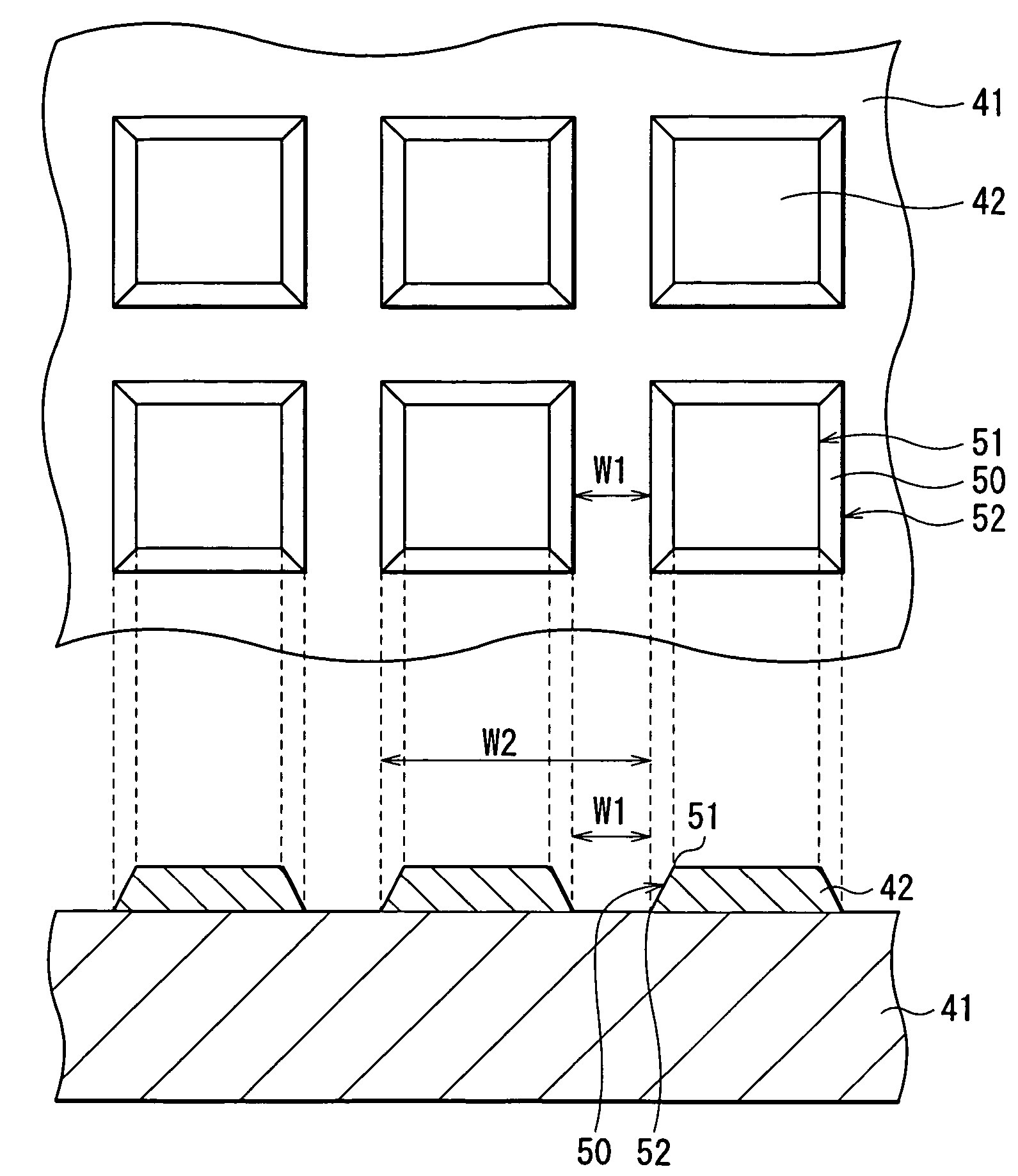
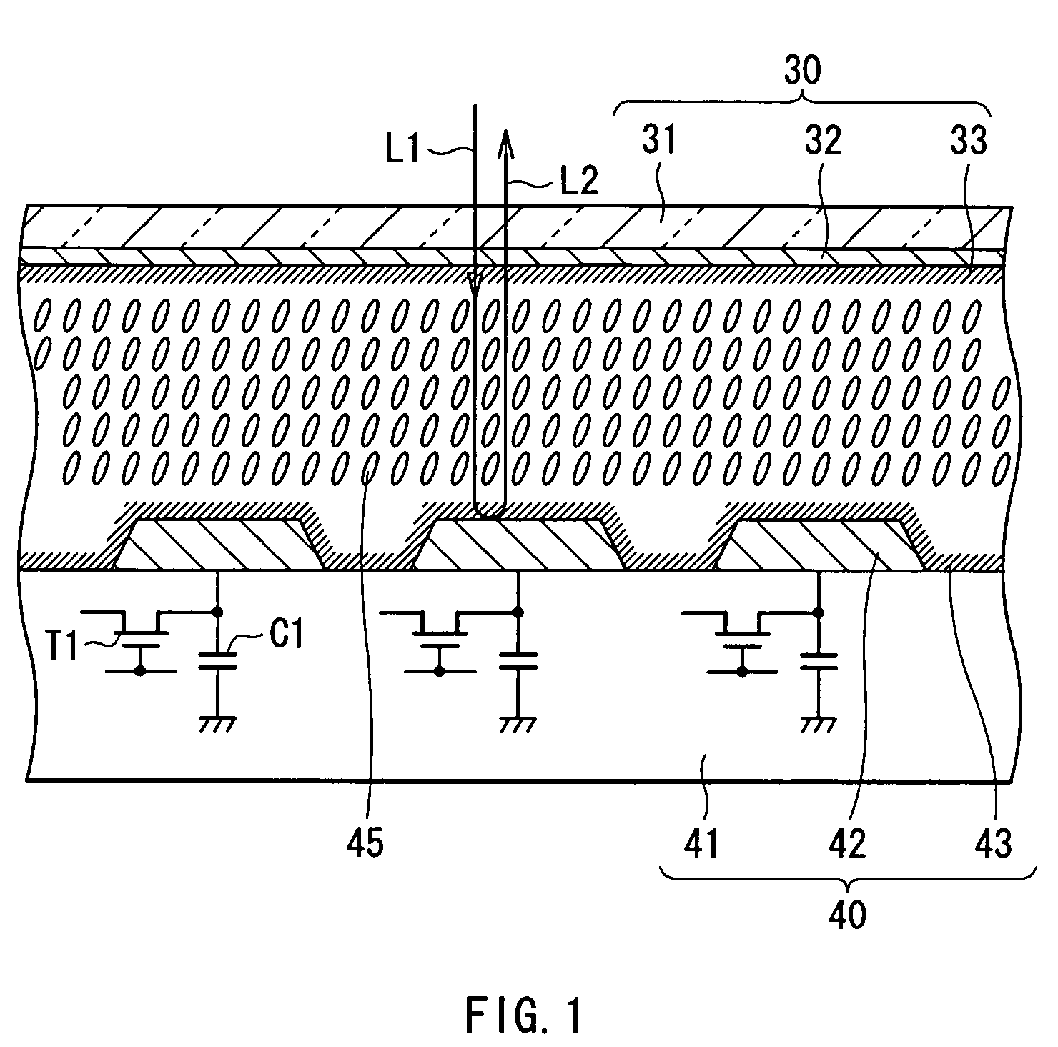
[0063]Basically, test samples of the reflective liquid crystal display device were formed according to the same method and the same specifications as those in the above comparative example. More specifically, after a glass substrate on which a transparent electrode was formed and a silicon drive substrate on which an aluminum electrode was formed as a reflective pixel electrode were cleaned, they were introduced into an evaporation apparatus to form a SiO2 film as an alignment film, and after that, a vertical liquid crystal material manufactured by Merck in which dielectric anisotropy Δ∈ was negative and the refractive index anisotropy Δn was 0.1 was injected between the substrates so as to form each of the test samples of the reflective liquid crystal display device. The reflective liquid crystal display devices in which the specifications of the silicon drive substrate were the same as those in the comparative example, and the pixel pitch W2 was 9 microns, and the width W1 between...
example 2
[0067]Test samples (test samples Nos. 21 through 25 in FIG. 8) of the reflective liquid crystal display device were formed through the same method as in Example 1. However, as a step of forming the pixel electrode, a process in which the surface of the pixel electrode was exposed to argon ions for a longer time than in Example 1 (100 seconds) was introduced. As a result, the structure in which a peripheral portion was substantially obliquely cut away by approximately 200 nm (corresponding to B=200 nm in FIG. 5) from the aluminum pixel electrode with a thickness of 150 nm (corresponding to A=150 nm in FIG. 5) was formed. It corresponded to B / A=1.33. The alignment state of the liquid crystal of each test sample with the pixel structure in the black level was observed by using through the same method as that in the comparative Example and Example 1.
[0068]The observation results are shown in FIG. 8. In the example, nonuniformity due to misalignment around the pixel groove which was obse...
PUM
| Property | Measurement | Unit |
|---|---|---|
| width | aaaaa | aaaaa |
| thickness | aaaaa | aaaaa |
| width W1 | aaaaa | aaaaa |
Abstract
Description
Claims
Application Information
 - R&D
- Intellectual Property
- Life Sciences
- Materials
- Tech Scout
- Unparalleled Data Quality
- Higher Quality Content
- 60% Fewer Hallucinations
Browse by: Latest US Patents, China's latest patents, Technical Efficacy Thesaurus, Application Domain, Technology Topic, Popular Technical Reports.
© 2025 PatSnap. All rights reserved.Legal|Privacy policy|Modern Slavery Act Transparency Statement|Sitemap|About US| Contact US: help@patsnap.com


