
Low-swing interconnections for field programmable gate arrays

a gate array and low-swing technology, applied in the field of integrated circuits, can solve problems such as dynamic power dissipation, and achieve the effects of reducing dynamic power consumption, maximizing performance, and reducing voltage swing

Active Publication Date: 2008-08-26
XILINX INC
View PDF7 Cites 13 Cited by
  • Summary
  • Abstract
  • Description
  • Claims
  • Application Information

AI Technical Summary

Benefits of technology

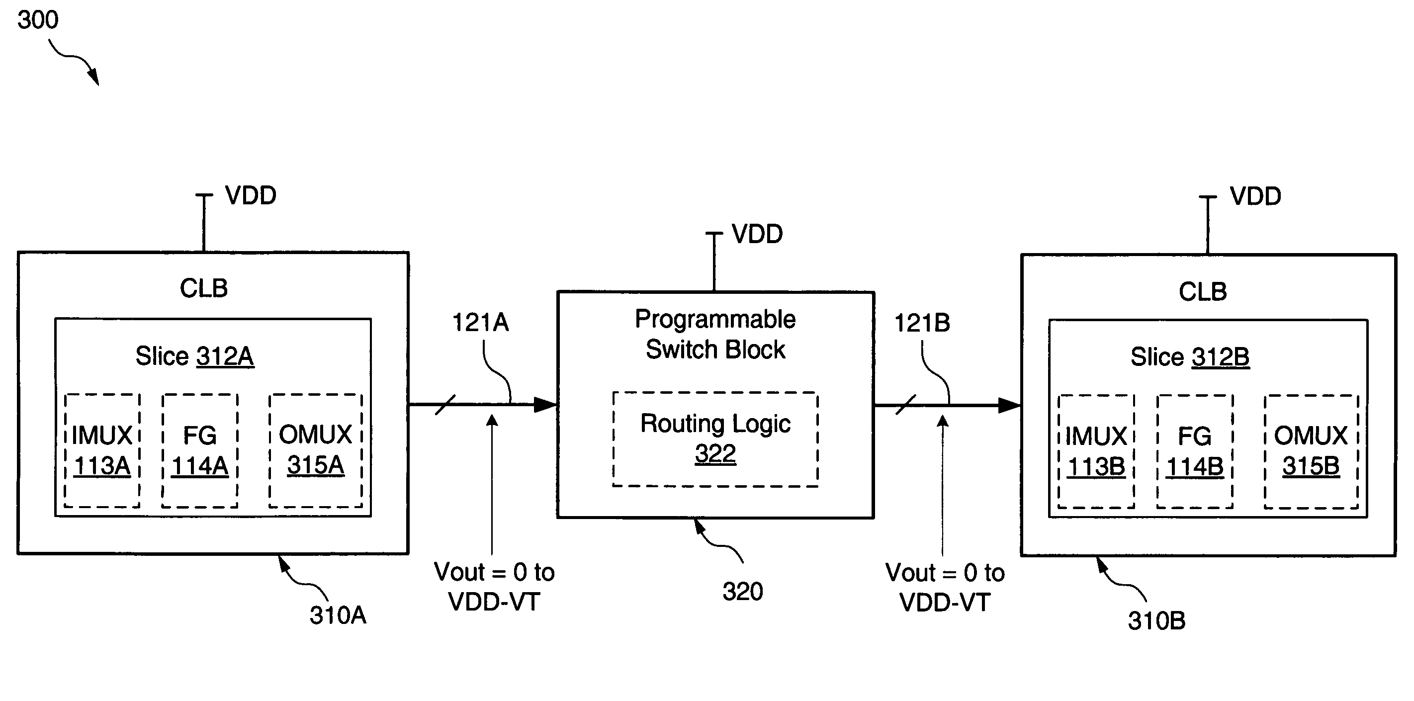
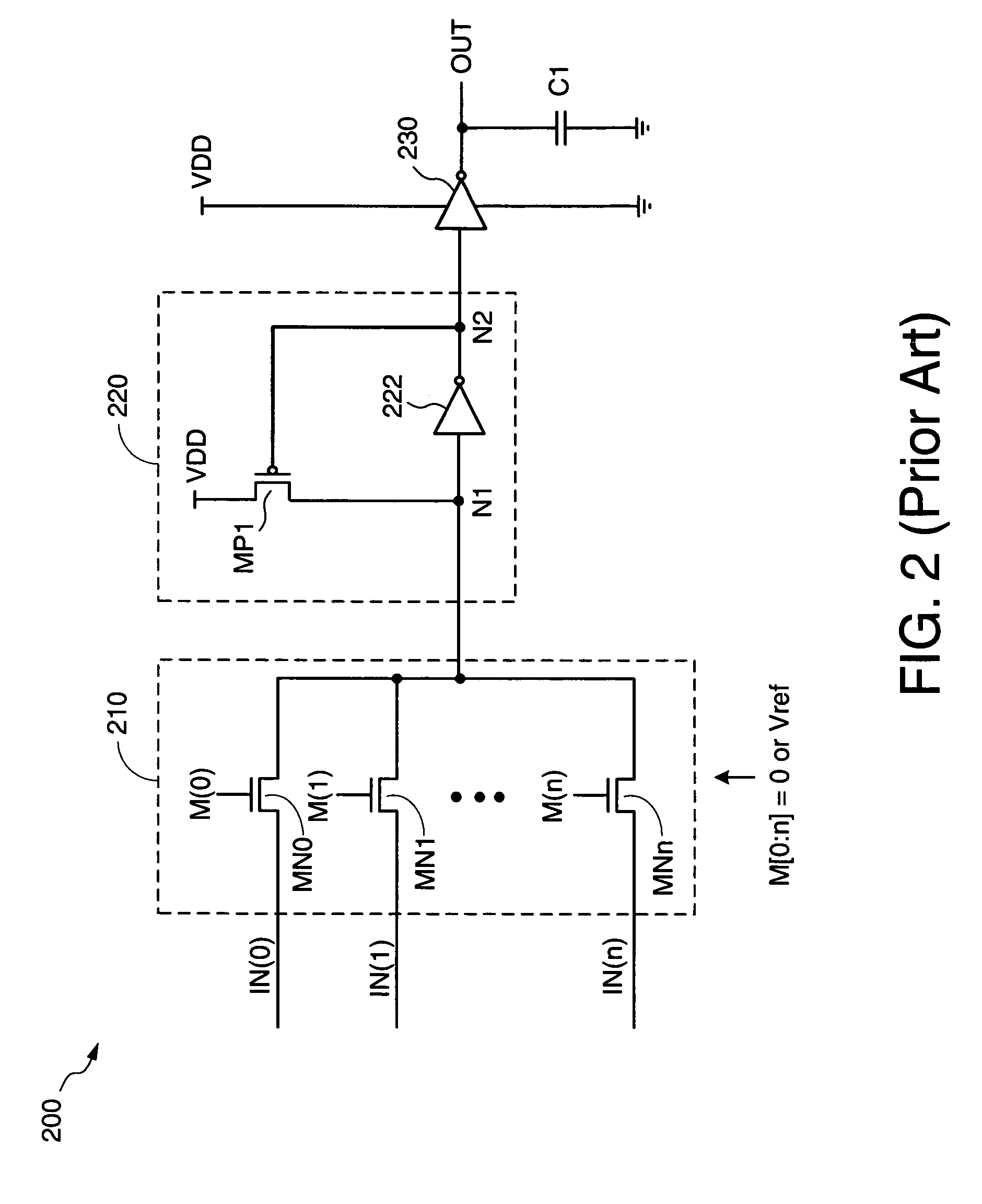
[0013]An apparatus is disclosed that may reduce the dynamic power dissipation of a configurable IC device such as an FPGA by reducing the peak-to-peak voltage swing of signals transmitted over the device's interconnect signal lines without including additional level shifter circuits. In accordance with some embodiments of the present invention, existing multiplexing circuit architectures provided within logic resources of various logic blocks of the configurable IC device may be used as level shifter circuits to increase the voltage swing of signals received into the blocks from the interconnect signal lines, and modified multiplexing circuit architectures provided within the logic resources may be used to reduce the voltage swing of signals output from the logic blocks onto the interconnect signal lines.
[0015]In operation, the input multiplexing circuit translates the voltage swing of logic signals received from the interconnect signal lines from a relatively low peak level to a relatively high peak level suitable for processing within the logic block's resources, and the output multiplexing circuit translates the voltage swing of logic signals received from the logic block's resources from a relatively high peak level to a relatively low peak level suitable for transmitting the signals over the interconnect signal lines. In this manner, embodiments of the present invention may reduce dynamic power consumption by reducing the voltage swing of signals transmitted over the interconnect signal lines while maximizing performance by increasing the voltage swing of signals to be processed within the logic blocks' resources.

Problems solved by technology

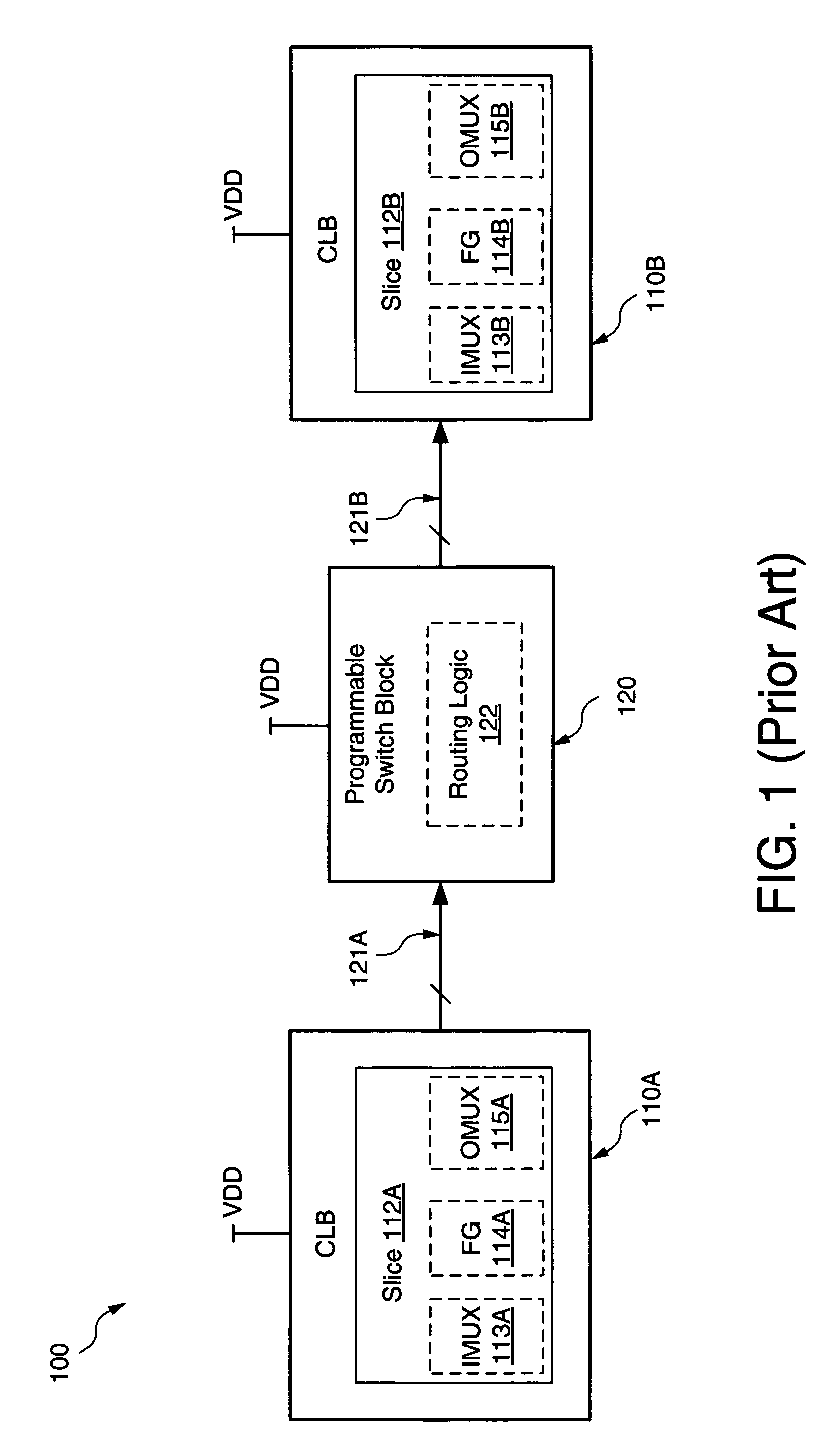
Each signal line in the FPGA's programmable interconnect structure has an associated wire capacitance that undesirably results in dynamic power dissipation when signals are routed over the interconnect signal lines.

Method used


Image

  • Low-swing interconnections for field programmable gate arrays
  • Low-swing interconnections for field programmable gate arrays
  • Low-swing interconnections for field programmable gate arrays

Examples


Embodiment Construction

[0028]Although described below in the context of an exemplary FPGA device, embodiments of the present invention are equally applicable to other configurable devices (e.g., various FPGA architectures and other programmable logic devices (PLDs) such as complex PLDs), including devices that may be partially configurable, and to other non-configurable devices (e.g., application-specific integrated circuits). In the following description, for purposes of explanation, specific nomenclature is set forth to provide a thorough understanding of the present invention. In other instances, well-known circuits and devices are shown in block diagram form to avoid obscuring the present invention. Further, the logic levels assigned to various signals in the description below are arbitrary and, thus can be modified (e.g., reversed polarity) as desired. Accordingly, the present invention is not to be construed as limited to specific examples described herein but rather includes within its scope all em...


PUM


Abstract

An apparatus is disclosed that may reduce the dynamic power dissipation of a configurable IC device such as an FPGA by reducing the peak-to-peak voltage swing of signals transmitted over the device's interconnect signal lines without including additional level shifter circuits. For some embodiments, existing multiplexing circuit architectures provided within logic resources of various logic blocks of the configurable IC device may be used as level shifter circuits to increase the voltage swing of signals received into the blocks from the interconnect signal lines, and modified multiplexing circuit architectures provided within the logic resources may be used to reduce the voltage swing of signals output from the logic blocks onto the interconnect signal lines.

Description

FIELD OF INVENTION[0001]The present invention relates generally to integrated circuits, and more specifically to shifting the voltage swing of signals transmitted between various resources of a configurable integrated circuit device.DESCRIPTION OF RELATED ART[0002]A configurable integrated circuit (IC) is an integrated circuit including various configurable resources. A programmable logic device (PLD) is a well-known type of configurable IC that can be programmed by a user to implement a variety of selected functions. PLDs are becoming increasingly popular with circuit designers because they require less time to design than custom-designed integrated circuits such as Application Specific Integrated Circuits (ASICs).[0003]There are many types of PLDs such as Field Programmable Gate Arrays (FPGAs) and complex PLDs (CPLDs). For example, an FPGA typically includes a plurality of configurable logic blocks (CLBs), a plurality of input / output blocks (IOBs), and a number of block RAM elemen...

Claims


Application Information

Patent Timeline
Patent Type & Authority Patents(United States)
IPC IPC(8): H03K19/173
CPCH03K19/17784H03K19/17728H03K19/1731H03K17/002H03K17/693
Inventor RAHMAN, ARIFURTUAN, TIMKAO, SEAN W.
Owner XILINX INC
Learn More