
Bias circuit for a wideband amplifier driven with low voltage

a bias circuit and amplifier technology, applied in the direction of amplifiers, amplifiers with semiconductor devices only, amplifiers with semiconductor devices, etc., can solve the problems of low power consumption, circuits cannot perform stable amplification operations at a reduced supply voltage, and it is difficult for conventional circuits to provide both amplification operations with a sufficiently high gain, and achieve low voltage operation.

Inactive Publication Date: 2008-07-08
LAPIS SEMICON CO LTD
View PDF2 Cites 16 Cited by
  • Summary
  • Abstract
  • Description
  • Claims
  • Application Information

AI Technical Summary

Benefits of technology

[0010]The bias circuit thus structured can provide a low voltage and low power consumption operation.

Problems solved by technology

The above-indicated amplifiers present, however, the following problems.
It is thus difficult for the circuit to provide a wide bandwidth operation of 500 MHz or more required by the UWB amplifiers.
The circuit cannot perform, however, a stable amplification operation at a reduced supply voltage.
More specifically, it is difficult for the conventional circuits to provide both of the amplification operation with a sufficiently high gain in the wideband and the amplification operation at a lower supply voltage.

Method used


Image

  • Bias circuit for a wideband amplifier driven with low voltage
  • Bias circuit for a wideband amplifier driven with low voltage
  • Bias circuit for a wideband amplifier driven with low voltage

Examples


Embodiment Construction

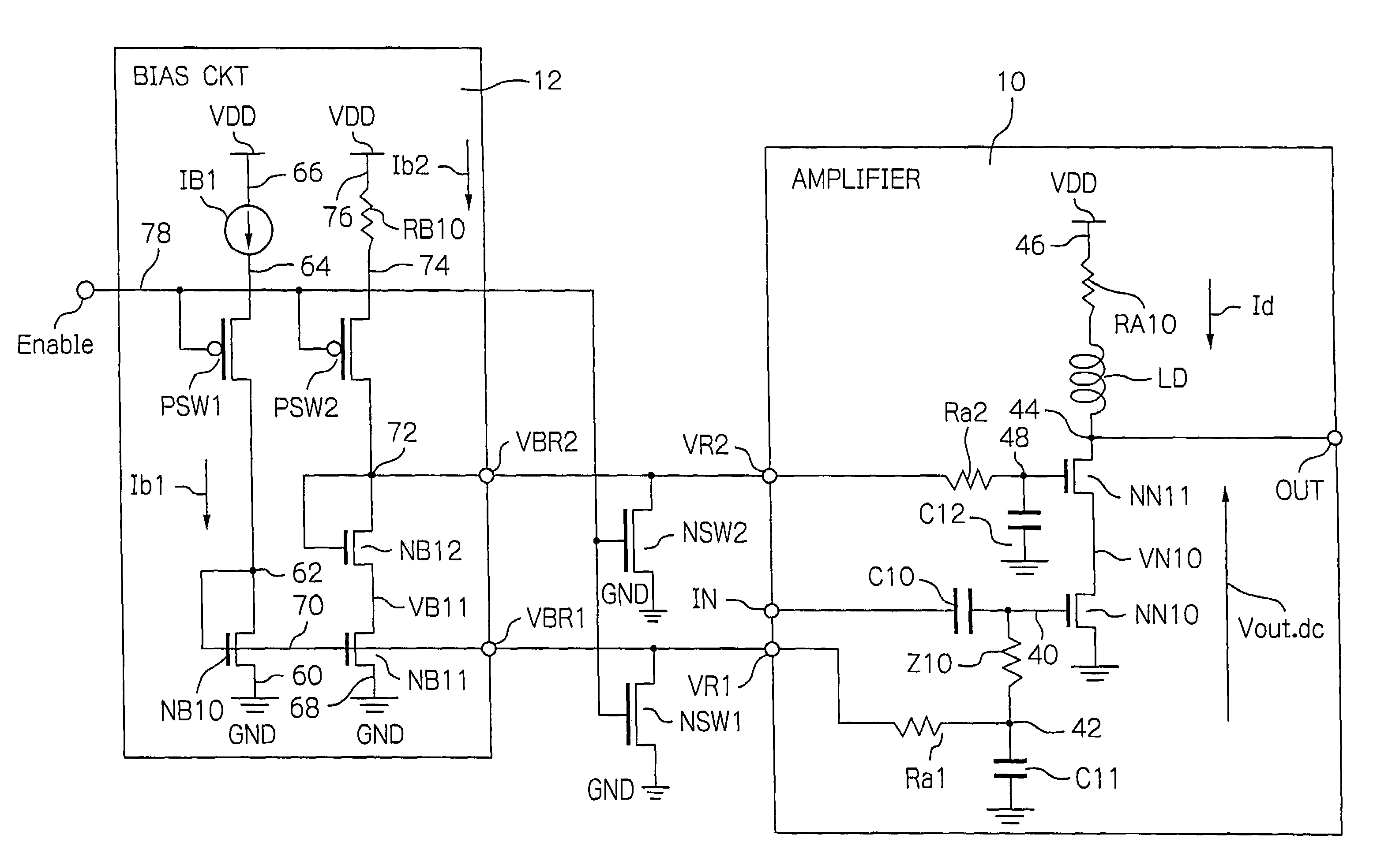
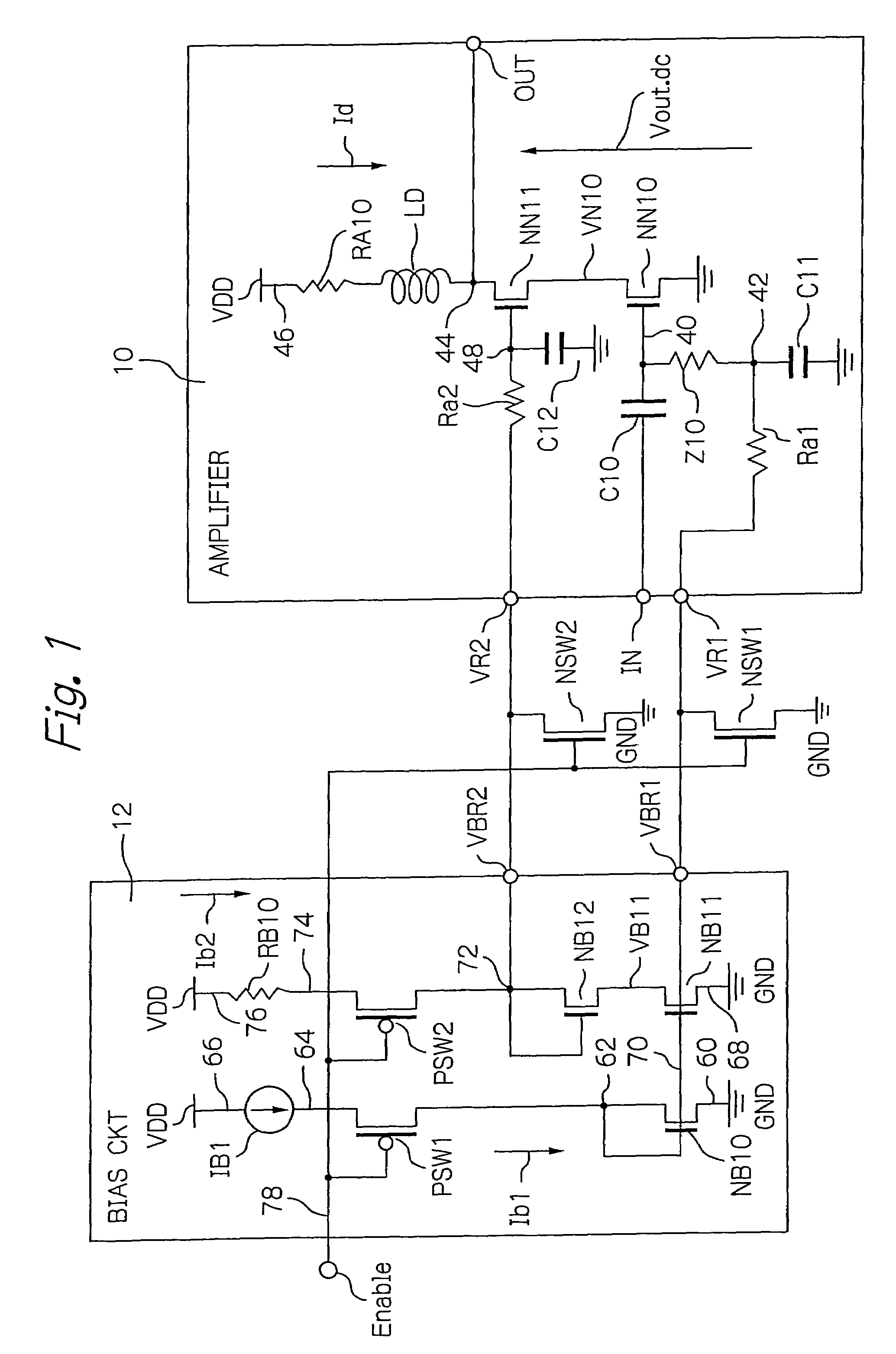
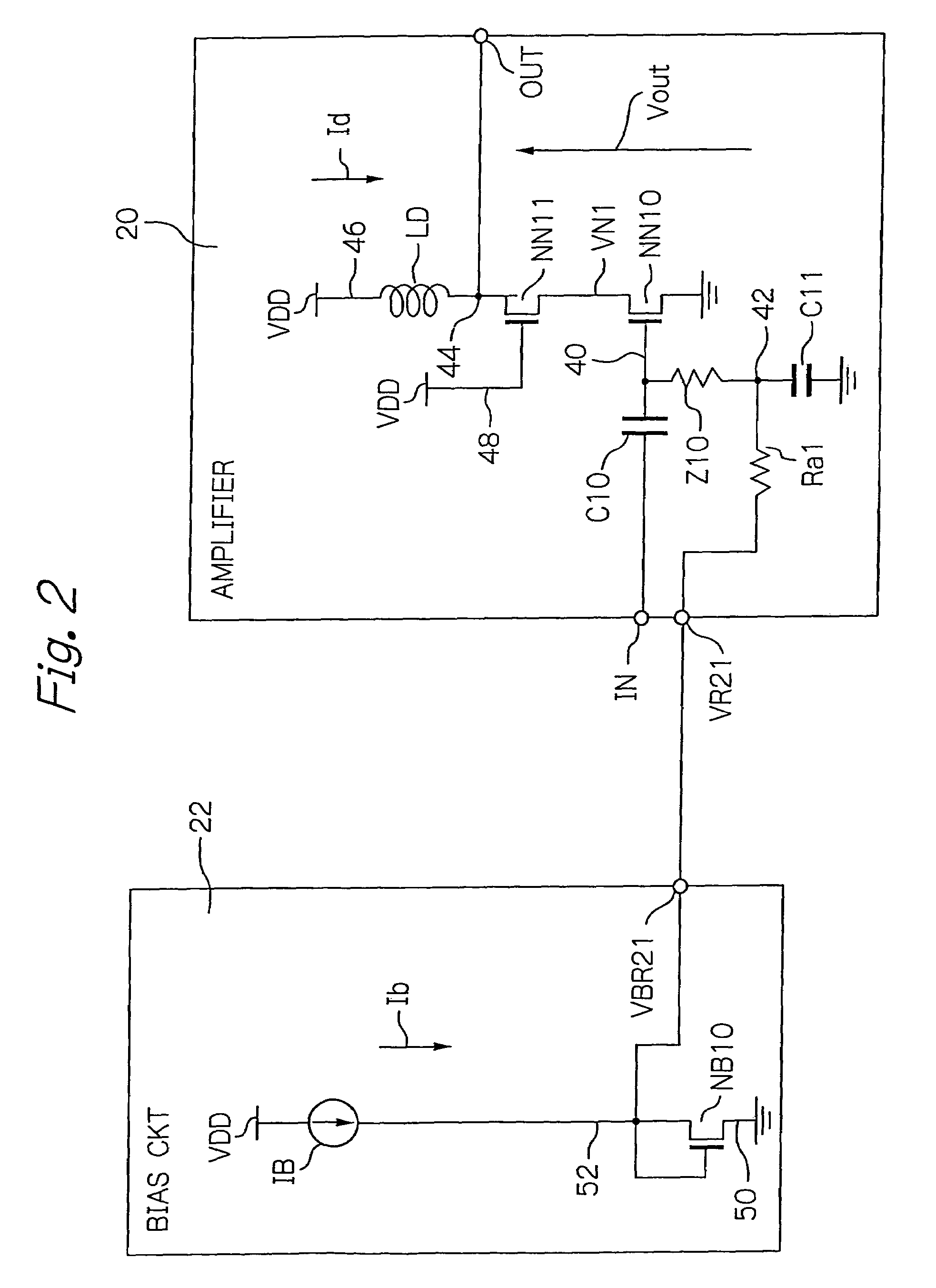
[0016]Referring now to accompanying drawings, embodiments of the bias circuit for an amplifier according to the present invention will be detailed below. Before the description of the embodiments of the present invention, for ease of understanding the present invention, a narrowband amplifier and a bias circuit for the amplifier and a wideband amplifier and a bias circuit for the amplifier will be described with reference to comparative examples shown in FIG. 2 and 3. The comparative example, the wideband amplifier, shown in FIG. 3 has a difficulty, compared to the present invention, in stable amplification operation at a lower supply voltage.

[0017]FIG. 2 shows a cascode type of high-frequency amplifier for use in the narrowband as a comparative example. The high-frequency amplifier has an amplifier 20 and a bias circuit 22 which are interconnected as illustrated. The amplifier 20 includes, for example, a source-grounded N-channel type metal-oxide semiconductor (NMOS) transistor NN1...


PUM


Abstract

An amplifier includes a ground, first and second MOS transistors, a first resistive load and a supply voltage, which are connected in series in this order. A bias circuit provides first and second bias voltages to the gate electrodes of the first and second transistors, respectively. The bias circuit includes a third MOS transistor having its gate and drain electrode diode-connected. The drain electrode of the third transistor provides the first bias voltage of the amplifier. The bias circuit further includes fourth and fifth MOS transistors, and a second resistive load, which are connected in series in this order. The second resistive load is connected to the supply voltage. The fourth transistor has its gate electrode connected to the drain electrode of the third transistor. The fifth transistor has its gate and drain electrodes diode-connected. The drain electrode of the fifth transistor provides the second bias voltage.

Description

BACKGROUND OF THE INVENTION[0001]1. Field of the Invention[0002]The present invention relates to a bias circuit for providing a bias voltage to a high-frequency amplifier. More specifically, the present invention relates to a bias circuit applicable to, for example, a so-called UWB (ultra wide band) amplifier, which requires operation in a wideband of 500 MHz or more.[0003]2. Description of the Background Art[0004]A conventional example of the high-frequency amplifier for use in a narrow band is disclosed in, for example, Thomas H. Lee, “The Design of CMOS Radio-Frequency Integrated Circuits,” Cambridge University Press, Cambridge, pp. 164-166 and pp. 288-292, 1998. This reference shows, on pages 164-166, an example of a cascode type amplifier for improving high frequency characteristics, and, on pages 288-292, an example of an amplifier with exemplified device constants.[0005]A conventional example of the high-frequency amplifier for use in a wide band is taught by, for example, Pa...

Claims


Application Information

Patent Timeline
Patent Type & Authority Patents(United States)
IPC IPC(8): H03F3/04
CPCH03F1/086H03F1/223H03F1/301H03F3/345H03F3/45183H03F3/04H03F2203/45508H03F2200/36H03F1/30
Inventor TANOI, SATORU
Owner LAPIS SEMICON CO LTD
Learn More