Oscillator and an integrated circuit

a technology of integrated circuits and oscillators, which is applied in the direction of oscillator generators, electrical equipment, etc., can solve the problems of noise and interference injection into the core of the oscillator, the damage of interference components, and the serious problem of large digital chips in the grounding of the oscillator, so as to achieve easy bias

Inactive Publication Date: 2008-04-22
TELEFON AB LM ERICSSON (PUBL)
View PDF7 Cites 9 Cited by
  • Summary
  • Abstract
  • Description
  • Claims
  • Application Information

AI Technical Summary

Benefits of technology

[0022]Additionally, the oscillator possesses excellent frequency shift performance, which allows the oscillator to be used in combination with other on-chip oscillators, e.g. RF oscillators, thus providing a stable reference frequency under all operational modes. The frequency shift performance can be measured as the change in frequency of the oscillator according to the present invention when interferers, like digital switching circuits or other oscillators, are switched on or off or when their operating conditions are otherwise changed. For the oscillator according to the present invention, the oscillation frequency is only affected by the interference to a very limited extent. This in turn makes it possible to comply with requirements concerning the variation of its output frequency without additional circuitry for reducing this variation. Test have shown that the present oscillator is able to fulfil the requirements set by the GSM / GPRS standards.
[0037]The invention also relates to an integrated circuit comprising a circuit which in combination with the resonator elements constitutes the oscillator as set forth above; said integrated circuit comprising terminals for electric interconnection with the resonator elements. Thereby, the components that take up a large area on the integrated circuit chip are arranged outside the integrated circuit chip. This is a more space- and cost-effective solution.

Problems solved by technology

A balanced structure as opposed to a single-ended structure helps, but even common-mode (i.e. exposures affecting both of a pair of balanced signals) interference components are also harmful.
This gain cell uses single-ended signals, and as a consequence, grounding of the oscillator is a severe problem for large digital chips.
This lack of sufficient grounding may result in noise and interference injection into the core of the oscillator.
Similarly, the integrated circuit substrate will not be connected directly to the resonator ground, thereby also providing an interference path into the circuit.
The above single-ended oscillators all suffer from not being sufficiently robust to substrate interference.
However, a drawback of this and other oscillators is a lack of robustness to the so-called substrate interference, which may originate in e.g. circuits on the same substrate involving intense digital switching, or other strong interference induced at the oscillator nodes, e.g. from another on-chip RF oscillator.
This imperfect performance results in small variations in the oscillation frequency, so called frequency shifts.
The GSM / GPRS requirements are more stringent than 1 ppm and, generally, this oscillator does not perform well enough with respect to the GSM / GPRS requirements.
As stated above, an integrated oscillator is prone to pick up substrate interference.
Furthermore, the drain has a parallel-plate capacitance to the substrate and this path may also cause noise injection.

Method used


Image

  • Oscillator and an integrated circuit
  • Oscillator and an integrated circuit
  • Oscillator and an integrated circuit

Examples


Embodiment Construction

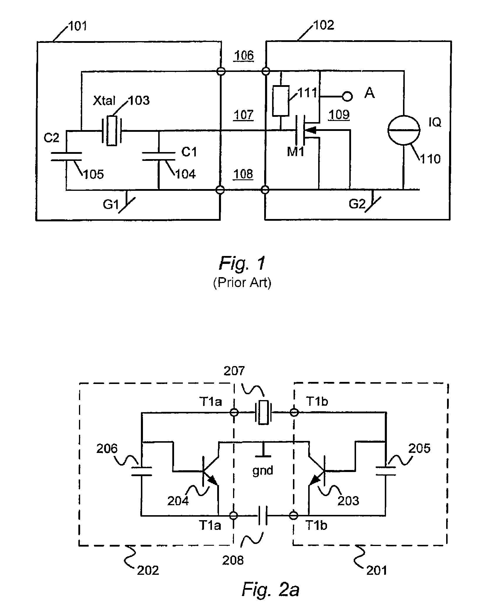
[0048]FIG. 1 shows a single-ended crystal oscillator. The oscillator circuit is illustrated to comprise a first and a second subcircuit. The first subcircuit 101 is typically implemented by means of passive components mounted on a printed circuit board (PCB), whereas the second subcircuit 102 is implemented on a substrate in an integrated circuit (IC) component that is mounted on the PCB.

[0049]The first subcircuit 101 comprises an oscillating device in the form of a crystal (Xtal) 103 for instance with a nominal oscillating frequency in the range of 10-40 MHz. The crystal is electrically connected to the second subcircuit 102 by means of two connectors 106 and 107.

[0050]At frequencies about the nominal series resonance frequency the crystal has relatively low impedance. However, at frequencies below and above the series resonance frequency the crystal has relatively high impedance. Thus, below and especially above the nominal frequency an oscillating signal across the crystal will b...


PUM


Abstract

A balanced crystal oscillator circuit comprising: a piezoelectric element Xtal (207; 215; 222,221; 313); a first oscillator subcircuit (202; 210; 218; 302) incorporating a transistor (204;212;220;304); and a second oscillator subcircuit (201;209;217; 301) incorporating a transistor (203; 211; 219; 303); wherein the transistors each have different types of transistor terminals (C,B,E; D;G;S), and wherein the oscillator subcircuits are configured with at least three interconnections. Each interconnection comprise a pair of like type of transistor terminals; wherein a first of said interconnections constitutes a connection to a ground reference (gnd); a second of said interconnections is via a first resonator element (207;215;223;313); and a third of said interconnections is via a second resonator element (208;216;224;314); said first and second circuits are arranged to interact by means of said first and second resonator elements to form a balanced oscillator signal. A dual common base or a dual common collector configuration is preferred.

Description

[0001]This patent application claims the benefit of priority from U.S. Provisional Patent Application Ser. No. 60 / 411,184 filed on Sep. 16, 2002. This application incorporates by reference the entire disclosure of U.S. Provisional Patent Application Ser. No. 60 / 411,184.TECHNICAL FIELD[0002]This invention relates to a balanced crystal oscillator circuit comprising: a piezoelectric element; a first oscillator subcircuit incorporating a transistor; and a second oscillator subcircuit incorporating a transistor; wherein the transistors each have different types of transistor terminals, and wherein the oscillator subcircuits are configured with at least three interconnections.BACKGROUND OF THE INVENTION[0003]A balanced crystal oscillator circuit can be employed in various electronic circuits. However, a special field of application is within communications equipment—especially telecommunications equipment—wherein frequency references are generated or synthesized as periodic signals for mo...

Claims


Application Information

Patent Timeline
Patent Type & Authority Patents(United States)
IPC IPC(8): H03B5/36H03B5/32
CPCH03B5/36H03B5/364H03B5/32
Inventor MATTISSON, SVEN
Owner TELEFON AB LM ERICSSON (PUBL)
Why Eureka
Try Eureka