Method of fabricating semiconductor integrated circuits

a technology of integrated circuits and semiconductors, applied in semiconductor/solid-state device testing/measurement, instruments, vacuum evaporation coating, etc., can solve the problems of high equipment cost, time-consuming, sectorial defect areas on wafers, etc., to achieve simple and effective production, the effect of promoting production yield

Active Publication Date: 2008-04-15
MARLIN SEMICON LTD
View PDF28 Cites 2 Cited by
  • Summary
  • Abstract
  • Description
  • Claims
  • Application Information

AI Technical Summary

Benefits of technology

[0008]It is therefore an object of the present invention to provide a simplified and more effective method for detecting the aforesaid sectorial defect areas particularly produced in the spin coat processes, thereby promoting production yields.

Problems solved by technology

The manufacture of integrated circuits requires high cost equipments, clean rooms and cutting edge process technologies.
Particles deposited on the wafer surface usually result in sectorial defect areas on the wafer, which are typically inspected by visual means.
Such manual process is done off-line, and is thus time consuming.
It is disadvantageous that according to this patent the wafer has to be removed from the wafer stage of a spin coat system and then placed on a conveyor driven by rollers, which moves the wafer linearly.
Besides, such inspection system is complicated and is not particularly effective in detecting the above-mentioned sectorial defect areas on the wafer.

Method used


Image

  • Method of fabricating semiconductor integrated circuits
  • Method of fabricating semiconductor integrated circuits
  • Method of fabricating semiconductor integrated circuits

Examples


Embodiment Construction

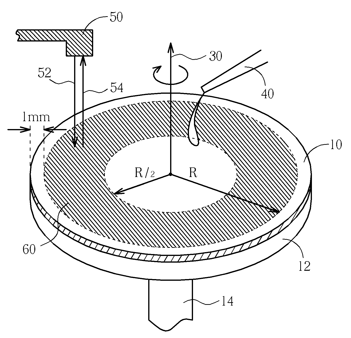
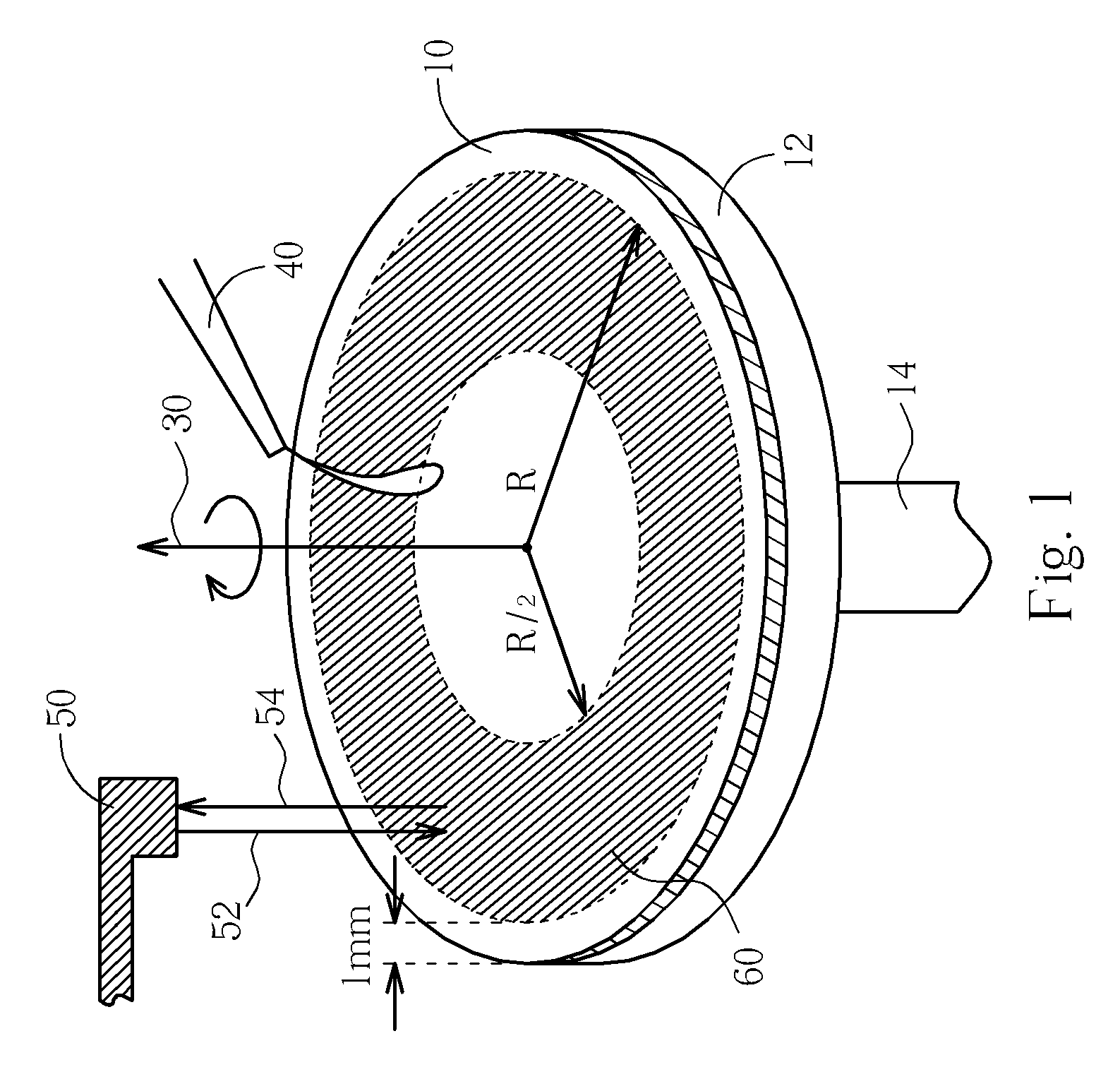
[0017]The present invention pertains to the non-contact measurement of film surface uniformity of a wafer, and is suited for any kinds of spin-on applications such as, for example, photoresist coatings, bottom / top anti-reflection coatings, spin-on glass, and low-k materials. It is essential to maintain the uniformity of a resist film's surface during or after the photoresist spin coating process since the uniformity of a resist film's surface can adversely affect pattern transfer accuracy in the subsequent exposure stage. As stated supra, particles deposited on the wafer surface usually result in sectorial defect areas on the wafer, which are typically inspected by visual means.

[0018]Referring to FIG. 1, a schematic diagram showing one preferred embodiment of the present invention is depicted. A wafer 10 with a radius R is disposed on a platen 12 of a spin-coating tool. The wafer 10 and the platen 12 driven by a shaft 14 together rotate about an axis 30. In some cases, the platen 12...


PUM

PropertyMeasurementUnit
radiusaaaaaaaaaa
radiusaaaaaaaaaa
threshold exposure energyaaaaaaaaaa

Abstract

A method of fabricating semiconductor integrated circuits includes (1) providing a spin-on tool comprising a rotatable platen for holding and spinning a wafer disposed thereon, a fluid supply system for providing spin-on solution onto the wafer, and a detector fixed in a position above the wafer, wherein the wafer has a radius R; (2) spin-on coating the wafer by depositing the spin-on solution onto surface of the wafer from its center and spinning-off to leave a spin coat material layer; and (3) spinning the wafer and scanning the spin coat material layer by impinging an incident light beam emanated from the fixed detector and detecting a reflected light beam.

Description

BACKGROUND OF INVENTION [0001]1. Field of the Invention[0002]The present invention relates generally to the fabrication of semiconductor integrated circuits and, more particularly, to a method of fabricating semiconductor integrated circuits with improved yields.[0003]2. Description of the Prior Art[0004]The manufacture of integrated circuits requires high cost equipments, clean rooms and cutting edge process technologies. To amortize this high capital expenditure, it is necessary to increase the yields as much as possible, but with costs for quality control and process realization at an acceptable level.[0005]Spin-on coated materials such as photoresists, spin-on glasses and some low-k materials are frequently used in this art. The spin-on material such as photoresist is dispensed onto a spinning wafer from its center. Particles deposited on the wafer surface usually result in sectorial defect areas on the wafer, which are typically inspected by visual means. For example, an operat...

Claims


Application Information

Patent Timeline
Patent Type & Authority Patents(United States)
IPC IPC(8): H01L21/47B05D3/12B05D5/12H01L21/312
CPCG01N21/9501H01L21/312H01L22/12H01L21/02282
Inventor WU, I-WENTSENG, CHEN-CHIU
Owner MARLIN SEMICON LTD
Why Eureka
Try Eureka