Light-emitting diode
a diode and light-emitting technology, applied in the direction of discharge tube/lamp details, discharge tube luminescnet screens, lighting and heating apparatus, etc., can solve the problems of insufficient luminance in many cases, and achieve the effects of preventing the leakage of light toward the back, enhancing the luminance on the surface in the optical axis direction, and increasing the contact area
- Summary
- Abstract
- Description
- Claims
- Application Information
AI Technical Summary
Benefits of technology
Problems solved by technology
Method used
Image
Examples
embodiment 1
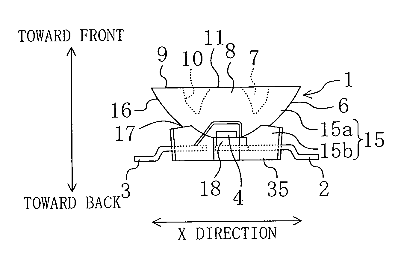
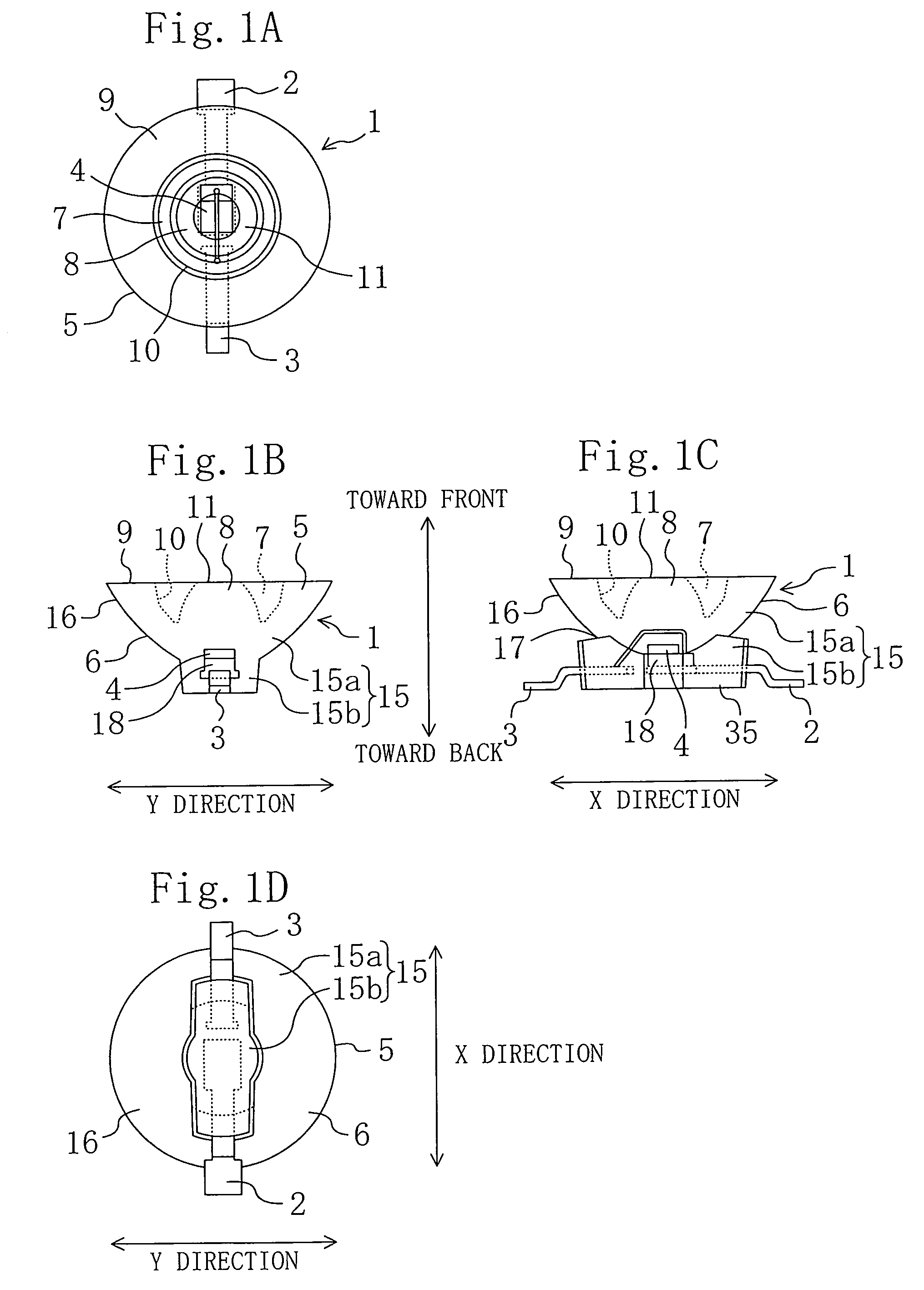
[0055]FIG. 1(A) is a plan view showing a light-emitting diode according to a first embodiment of the present invention. FIG. 1(B) is a front view of the light-emitting diode. FIG. 1(C) is a side view of the light-emitting diode. FIG. 1(D) is a bottom view of the light-emitting diode.
[0056]As shown in FIG. 1, a light-emitting diode 1 includes: a semiconductor light-emitting device 4 mounted over lead frames 2 and 3; and a transparent resin package 5 covering the semiconductor light-emitting device 4.
[0057]The lead frames 2 and 3 are formed by bending, into a gull-wing shape, a plate member obtained by, for example, applying a Ni / Ag coating to a Cu alloy or others. More specifically, the lead frames 2 and 3 extend from base parts thereof over which the semiconductor light-emitting device 4 is mounted, project from both sides of the resin package 5, bend backward and then outward, and extend to the outside at the both sides.
[0058]The semiconductor light-emitting device 4 in the shape o...
embodiment 2
[0086]FIG. 3(A) is a plan view showing a light-emitting diode according to a second embodiment of the present invention. FIG. 3(B) is a front view of the light-emitting diode. FIG. 3(C) is a side view of the light-emitting diode. FIG. 3(D) is a bottom view of the light-emitting diode.
[0087]A light-emitting diode 22 according to the second embodiment is different from the light-emitting diode 1 of the first embodiment in that two semiconductor light-emitting devices and four lead frames are provided.
[0088]Lead frames 23, 24, 25 and 26 are formed into gull-wing shapes and are arranged close to each other at an end and form a cross. Two semiconductor light-emitting devices 27 and 28 are respectively mounted over the opposed lead frames 23 and 25 by die bonding. The semiconductor light-emitting device 27 is connected to the lead frame 25 by wire bonding. The semiconductor light-emitting device 28 is connected to the lead frame 26 by wire bonding. The centers of the respective semiconduc...
embodiment 3
[0099]In a third embodiment, though not shown, a light-emitting diode in which three semiconductor light-emitting devices are mounted over lead frames will be described. The light-emitting diode according to this embodiment uses semiconductor light-emitting devices emitting red light, green light and blue light, respectively. Each of the semiconductor light-emitting devices can produce one of red, green and blue, a mixture of two of these colors, or a mixture of these three colors. White light can also be produced by adjusting the luminances of the three colors.
[0100]In this embodiment, a circular flat portion is formed on each convex lens portion to diffuse light, so that the luminances of the colors are made uniform and the colors are uniformly mixed.
[0101]White light obtained from blue light by using a yellow phosphor has a small amount of red component. Accordingly, if such white light is used by a flash for taking pictures, white light different from natural light is generated....
PUM
 Abstract
Description
Claims
Application Information
 - R&D
- Intellectual Property
- Life Sciences
- Materials
- Tech Scout
- Unparalleled Data Quality
- Higher Quality Content
- 60% Fewer Hallucinations
Browse by: Latest US Patents, China's latest patents, Technical Efficacy Thesaurus, Application Domain, Technology Topic, Popular Technical Reports.
© 2025 PatSnap. All rights reserved.Legal|Privacy policy|Modern Slavery Act Transparency Statement|Sitemap|About US| Contact US: help@patsnap.com


