Optical modulator and optical modulating method
a technology of optical modulator and optical modulator, which is applied in the direction of optical elements, using reradiation, instruments, etc., can solve the problems of deteriorating reducing the 3-db-down bandwidth, and affecting the operation efficiency of the optical modulator. , to achieve the effect of widening the operation bandwidth, shortening the device length, and improving the flatness of the frequency characteristic of the e/o respons
- Summary
- Abstract
- Description
- Claims
- Application Information
AI Technical Summary
Benefits of technology
Problems solved by technology
Method used
Image
Examples
first embodiment
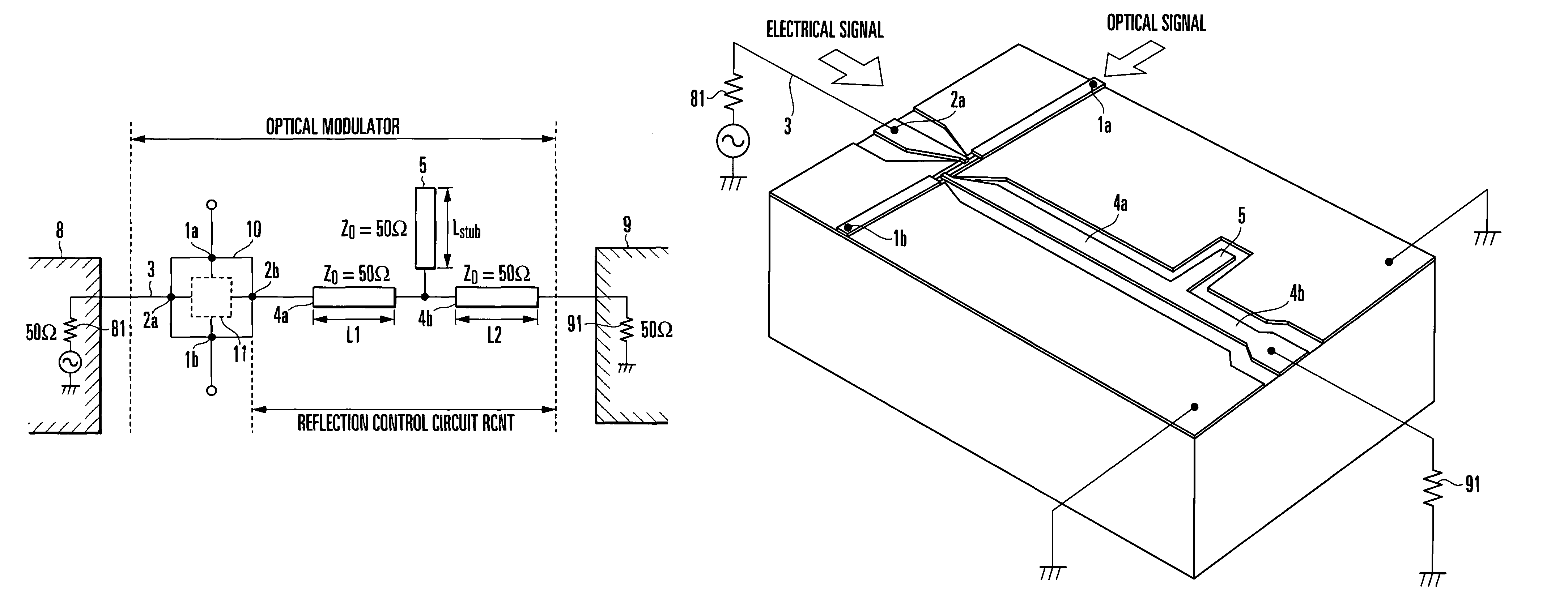
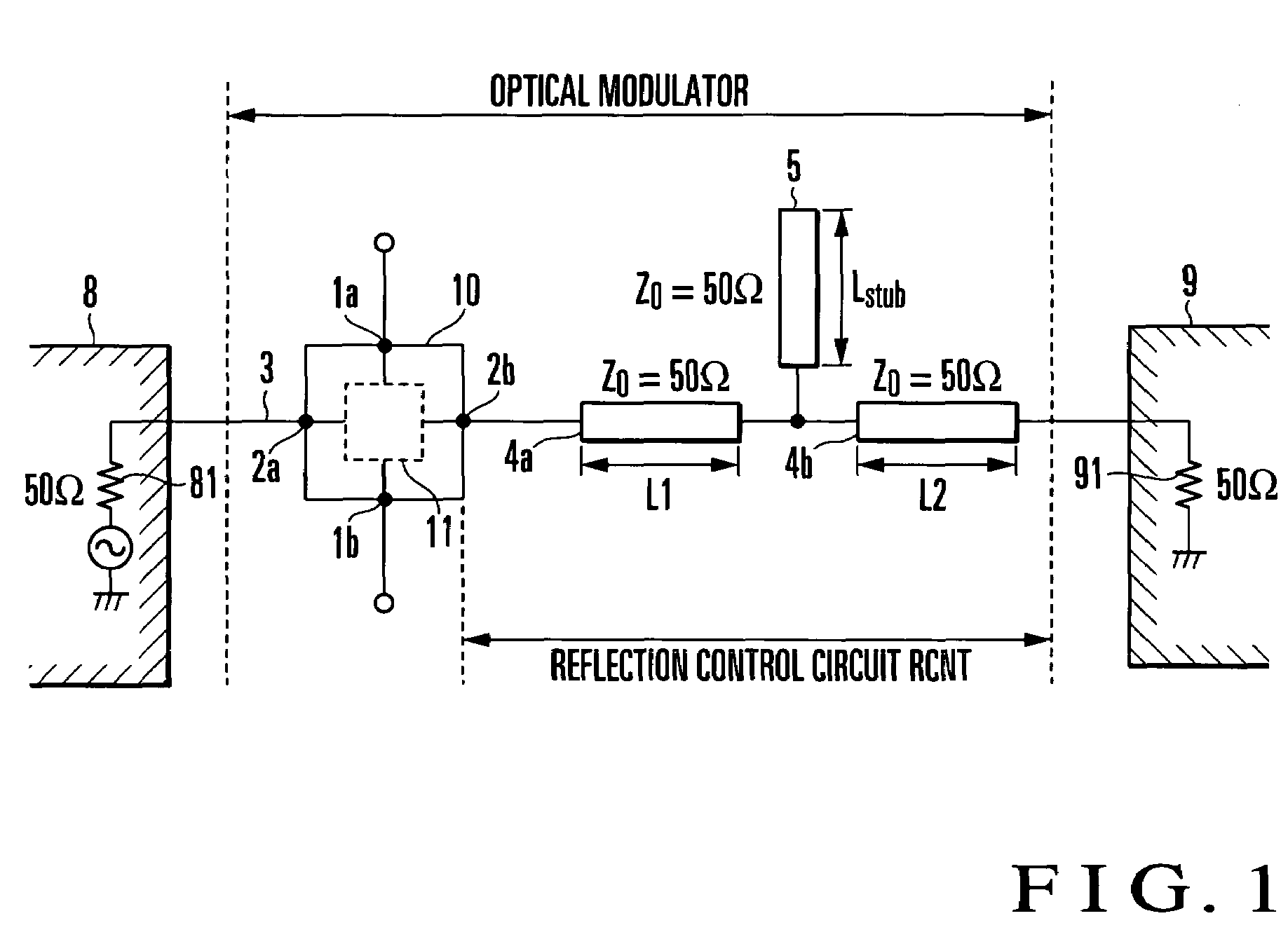
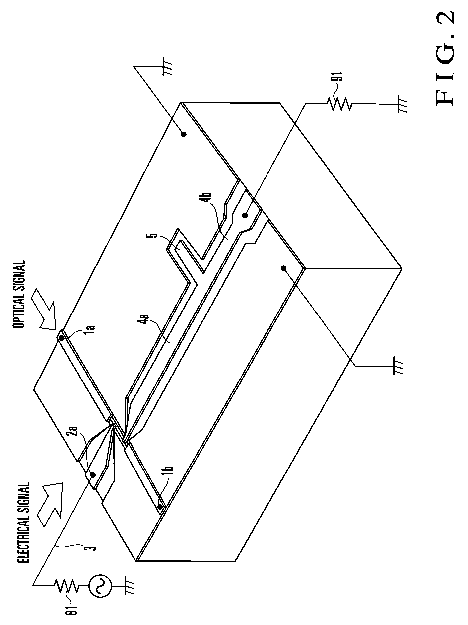
[0061]FIG. 1 shows the first embodiment of an optical modulator of the present invention, and this optical modulator has an optical modulation device 10 including an optical signal input terminal 1a, an optical signal output terminal 1b, an electrical signal input terminal 2a, an electrical signal output terminal 2b, and an electrical / optical interaction region 11 in which input optical and electrical signals interact with each other.
[0062]Also, a first electrical signal line 3 is connected to the electrical signal input terminal 2a of the optical modulation device 10 described above, and a second electrical signal line 4a which forms a part of a refection control circuit RCNT is connected to the electrical signal output terminal 2b.
[0063]An (equivalent) input terminating resistor 81 on the input terminating side 8 of an electrical signal driving system is connected to the first electrical signal line 3.
[0064]The reflection control circuit RCNT is placed between the optical modulat...
second embodiment
[0088]The second embodiment of the present invention will be described below with reference to FIG. 9.
[0089]In the first embodiment, a reflected electrical signal is generated by connecting the impedance component in parallel to the electrical signal output side of the optical modulation unit. In this embodiment, a reflected electrical signal is generated by connecting an inductive reactance as a reflection control circuit RCNT in series with the electrical signal output side of an optical modulation unit.
[0090]FIG. 9 shows the arrangement of an optical modulator according to this embodiment, in which the same reference numerals as in FIG. 1 denote the same components as the optical modulator shown in FIG. 1, and an explanation thereof will be appropriately omitted.
[0091]As shown in FIG. 9, an element 71 connected in series with a second electrical signal line 4 is an inductor. Letting L be the inductance value and ω be the angular frequency, the element 71 has an inductive reactanc...
third embodiment
[0096]The third embodiment of the present invention will be described below with reference to FIG. 12.
[0097]This embodiment is equivalent to an arrangement in which as a reflection control circuit RCNT, a reactance is connected in parallel to and an element 71 (an inductive reactance) is connected in series with the electrical signal output side of an optical modulation unit, i.e., equivalent to a combination of the first and second embodiments described above.
[0098]FIG. 12 shows the arrangement of an optical modulator according to this embodiment, in which the same reference numerals as in FIG. 1 denote the same components as the optical modulator shown in FIG. 1, and an explanation thereof will be appropriately omitted. A practical example is shown in FIG. 13, in which an optical modulation device 10 and the reflection control circuit RCNT are separately formed, and connected by bonding wires 711a to 711c. In this practical example shown in FIG. 13, series transmission lines 4a an...
PUM
| Property | Measurement | Unit |
|---|---|---|
| resistance value | aaaaa | aaaaa |
| impedance | aaaaa | aaaaa |
| impedance Z0 | aaaaa | aaaaa |
Abstract
Description
Claims
Application Information
 - R&D
- Intellectual Property
- Life Sciences
- Materials
- Tech Scout
- Unparalleled Data Quality
- Higher Quality Content
- 60% Fewer Hallucinations
Browse by: Latest US Patents, China's latest patents, Technical Efficacy Thesaurus, Application Domain, Technology Topic, Popular Technical Reports.
© 2025 PatSnap. All rights reserved.Legal|Privacy policy|Modern Slavery Act Transparency Statement|Sitemap|About US| Contact US: help@patsnap.com


