Optical package with double formed leadframe

a leadframe and optical package technology, applied in the field of optical package, can solve the problems of high cost, high cost of mold design and construction, and use of the top side of the die pad of the leadframe, and achieve the effects of low cost, easy and less expensive to make, and low cos

Active Publication Date: 2008-03-18
VISHAY CAPELLA MICROSYST TAIWAN LTD
View PDF4 Cites 1 Cited by
  • Summary
  • Abstract
  • Description
  • Claims
  • Application Information

AI Technical Summary

Benefits of technology

[0007]It is accordingly an object of the present invention to provide a method and a package for semiconductor chips, in particular a clean mode package (CMP) for an optical system, which overcomes the hereinbefore-mentioned disadvantages of the known prior art with additional cost and low reliability. Without adding supplementary components and modifying the specification of a mold which bends fingers of leadframes, the packages of the present invention are easier and less expensive to make than conventional plastic packages, and are more reliable and efficiently-sized than conventional packages.
[0009]In accordance to the preferred embodiment of the present invention, a method employing the bottom surface of the die pad is disclosed. The term “double formed leadframe” means a leadframe not only utilizing the top surface of the die pad but also employing the bottom surface of the die pad. A metal leadframe includes a substantially planar die pad within and connected to the leadframe. A plurality of finger-like tabs extends from the leadframe toward the die pad without contacting the die pad. The number and location of the tabs around the frame may vary. Silver colloid is applied on the bottom surface of the die pad of the leadframe and a portion of the lead fingers. At least one semiconductor die is placed on the die pad of the leadframe. The surface of the substrate of the semiconductor die is attached on the adhesive silver colloid layer applied on the bottom surface of the die pad of the leadframe. Generally, there are multiple pads on the top surface of the semiconductor die. Those pads are formed by creating multiple rectangular window areas on the top isolation layer of the semiconductor die so that the top metal layer of the semiconductor die can be reached by the bonding wires. A plurality of bond wires electrically provides connections between the pads on the semiconductor die and the portion of lead fingers deposited with a layer of silver colloid. Silver colloid material increases the reliability for the binding between bond wires and lead fingers of the leadframe. Also, silver colloid material provides an adhesive layer and a grounding layer for the semiconductor die. The adhesive layer settles the semiconductor die on the die pad of the leadframe and the grounding layer helps the semiconductor die with good electrical characteristics by providing a grounding path for noise in the substrate.

Problems solved by technology

Generally, it is costly to design and construct a mold and it is hard to modify the specification of a mold.
A problem with conventional CMP is that only the top side of a die pad of a leadframe is utilized.
The oxidation of the metal material of socket and the solderable materials causes deterioration of the reliability.
Although the other side of the mother printed circuit board is employed, cost for a system with additional daughter printed circuit board increases and reliability for a system connecting a complex component decreases.

Method used


Image

  • Optical package with double formed leadframe
  • Optical package with double formed leadframe
  • Optical package with double formed leadframe

Examples


Embodiment Construction

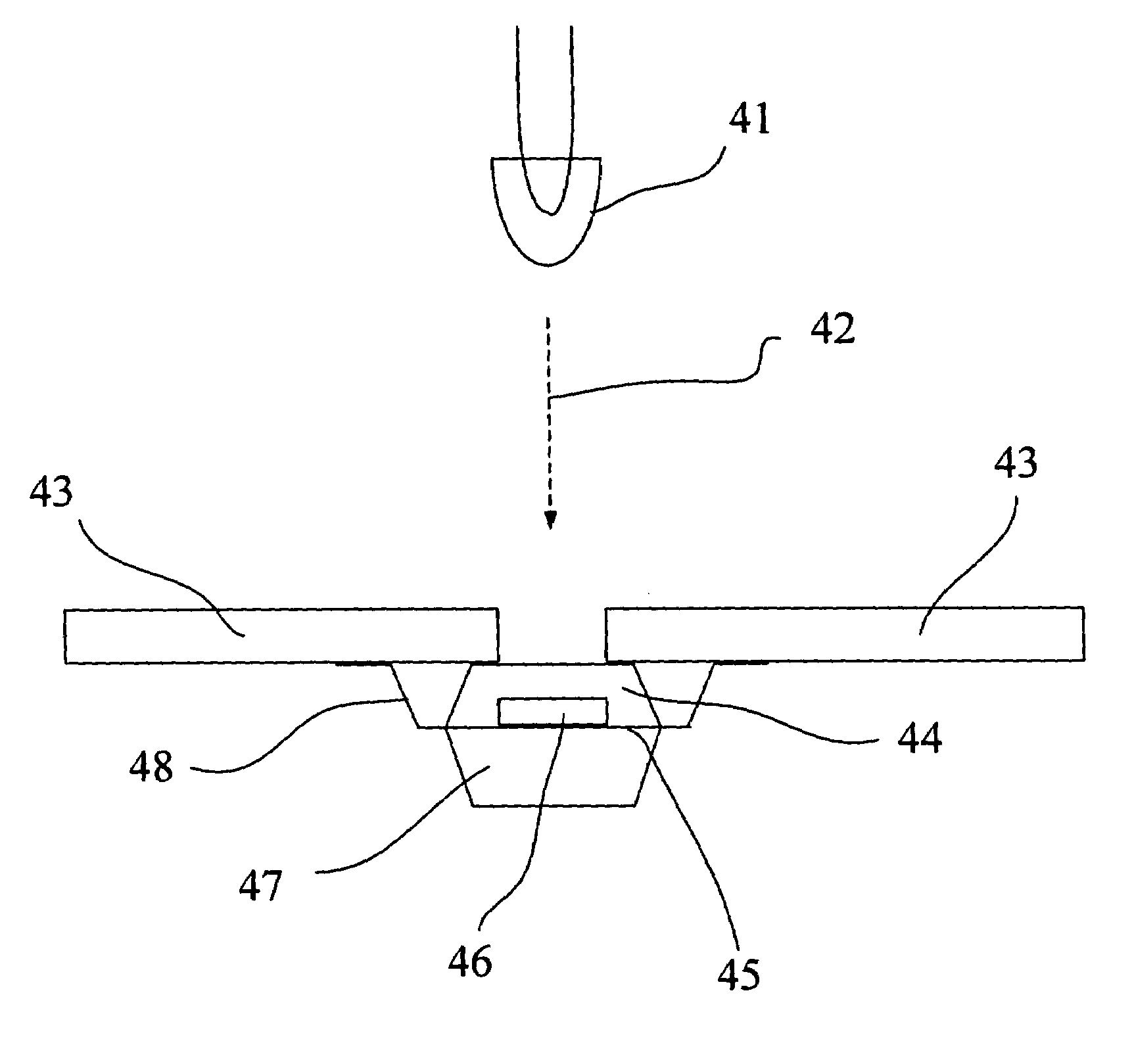
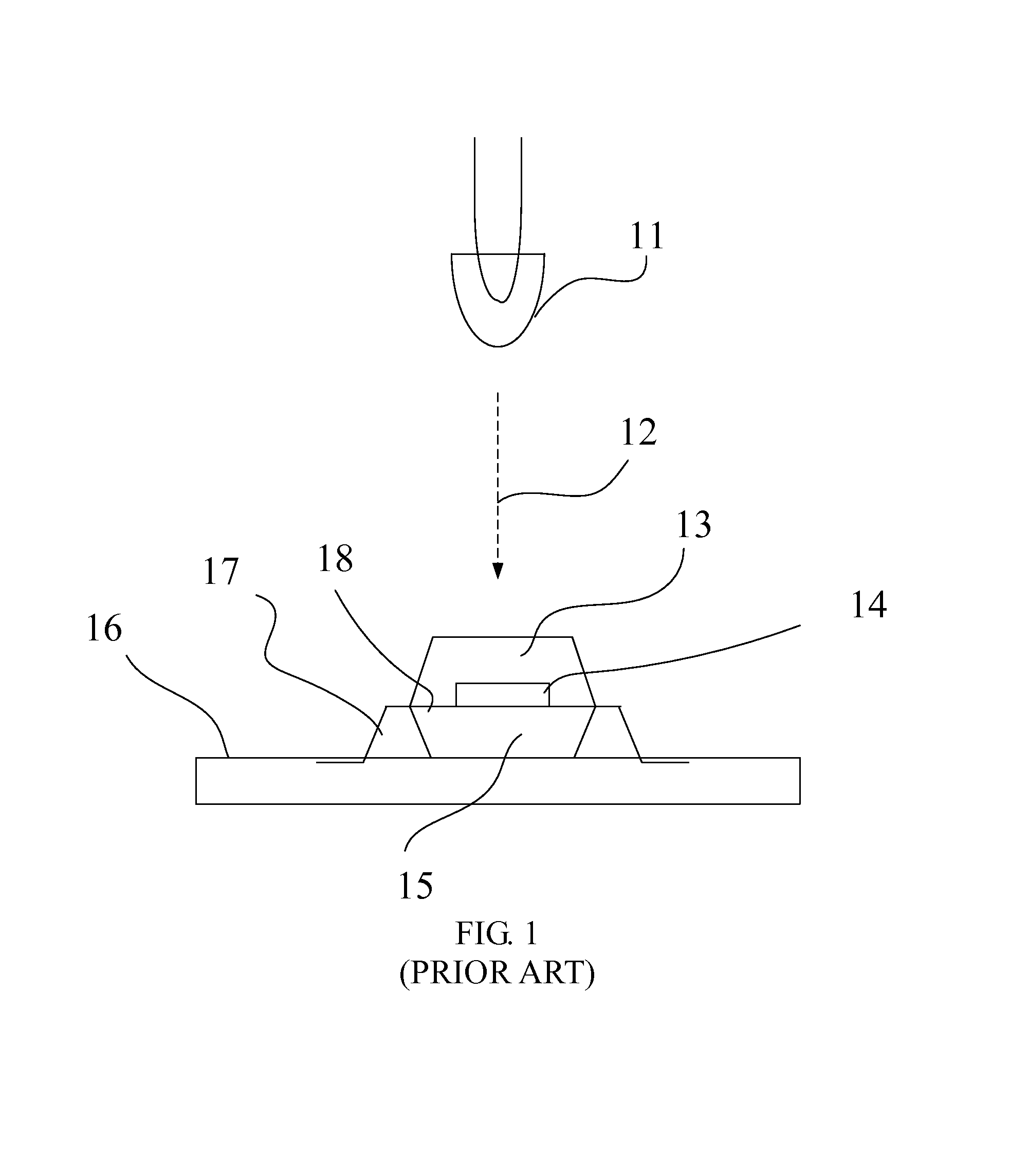
[0022]FIG. 1 is a cross-sectional diagram of an optical system in prior art. A leadframe including a substantially planar die pad 18 within and connected to the leadframe has multiple lead fingers 17 at specific bending angles, wherein a portion of the lead fingers is mounted on a top surface of a printed circuit board 16. There is an integrated circuit die 14 attached on the upward first pad surface of the leadframe. A top encapsulating dielectric material 13 is applied onto the upward first pad surface and a bottom encapsulating dielectric material 15 onto a downward second pad surface. The top encapsulating dielectric material 13 also embraces the integrated circuit die 14 and a portion of the multiple lead fingers 17. Generally, the encapsulating dielectric material 13 is transparent for a package embodied an optical integrated circuit die 14, wherein the optical integrated circuit die 14 receives the optical information 12 from environment outside, manipulates the variation of ...


PUM


Abstract

Packages for an optical integrated circuit die and a method for making such packages are disclosed. The package includes a die, a die pad, a plurality of lead fingers, and an encapsulating dielectric material. The downward second pad surface of the die pad bearing an integrated circuit is encapsulated by a bottom encapsulating dielectric material. The top encapsulating dielectric material provides the function for protecting the leadframe from severe environment. The top encapsulating dielectric material can be neglected if there is no threat on the integrated circuit die and the leadframe. Multiple of lead fingers are mounted on the printed circuit board. A portion of the printed circuit board is removed in order to provide an optical path for the light beam transmitted from a light source through the transparent bottom encapsulating dielectric material into the integrated circuit die. The method of making a package includes forming a leadframe including a die pad and a plurality of lead fingers. A die is attached on the downward second surface of the die pad. There are bonding wires electrically coupling the die and the lead fingers. Transparent dielectric encapsulating material covers the die, the die pad and a portion of the lead fingers. Finally, the package is mounted on a printed circuit board with flatly bended tip portion of the lead fingers.

Description

REFERENCE TO RELATED APPLICATION[0001]This Application is based on U.S. Provisional Patent Application Ser. No. 60 / 696,822 filed on 7 Jul. 2005.FIELD OF THE INVENTION[0002]The present invention relates to an IC package and a method for making the same. More particularly, the invention relates to leadframe structures and methods for using in optical systems.BACKGROUND OF THE INVENTION[0003]The package is to toward a cost oriented business of manufacturing. Generally, an integrated circuit die is enclosed in plastic packages to be resistant to hostile environments and to provide electrical connections between the semiconductor die and printed circuit boards. A package usually includes a metal leadframe, a semiconductor die, bonding material to attach the semiconductor die to the leadframe, bonding wires connecting pads on the semiconductor die to lead fingers of the leadframe, and a plastic encapsulant material sheltering all the components mentioned above but a portion of lead finger...

Claims


Application Information

Patent Timeline
Patent Type & Authority Patents(United States)
IPC IPC(8): H01L23/495
CPCH01L23/3107H01L2924/1532H01L2224/48091H01L2924/00014H01L2224/48247H01L2924/181H01L2924/00012
Inventor CHIEN, CHIH-CHENG
Owner VISHAY CAPELLA MICROSYST TAIWAN LTD
Why Eureka
Try Eureka