
Bidirectional current-mode transceiver

a current-mode transceiver and current-mode technology, applied in the direction of logic circuit coupling/interface arrangement, digital transmission, pulse technique, etc., can solve the problems of delay of logic gate, time delay, and greater delay of transmission line, and achieve long transmission line, large area, and great power consumption

Inactive Publication Date: 2008-03-11
IND TECH RES INST
View PDF3 Cites 6 Cited by
  • Summary
  • Abstract
  • Description
  • Claims
  • Application Information

AI Technical Summary

Benefits of technology

The bidirectional current-mode transceiver effectively addresses the issues of delay and power consumption by improving transmission rates on long transmission lines, reducing voltage swing, and simplifying circuit design, making it suitable for applications where conventional methods are inadequate.

Problems solved by technology

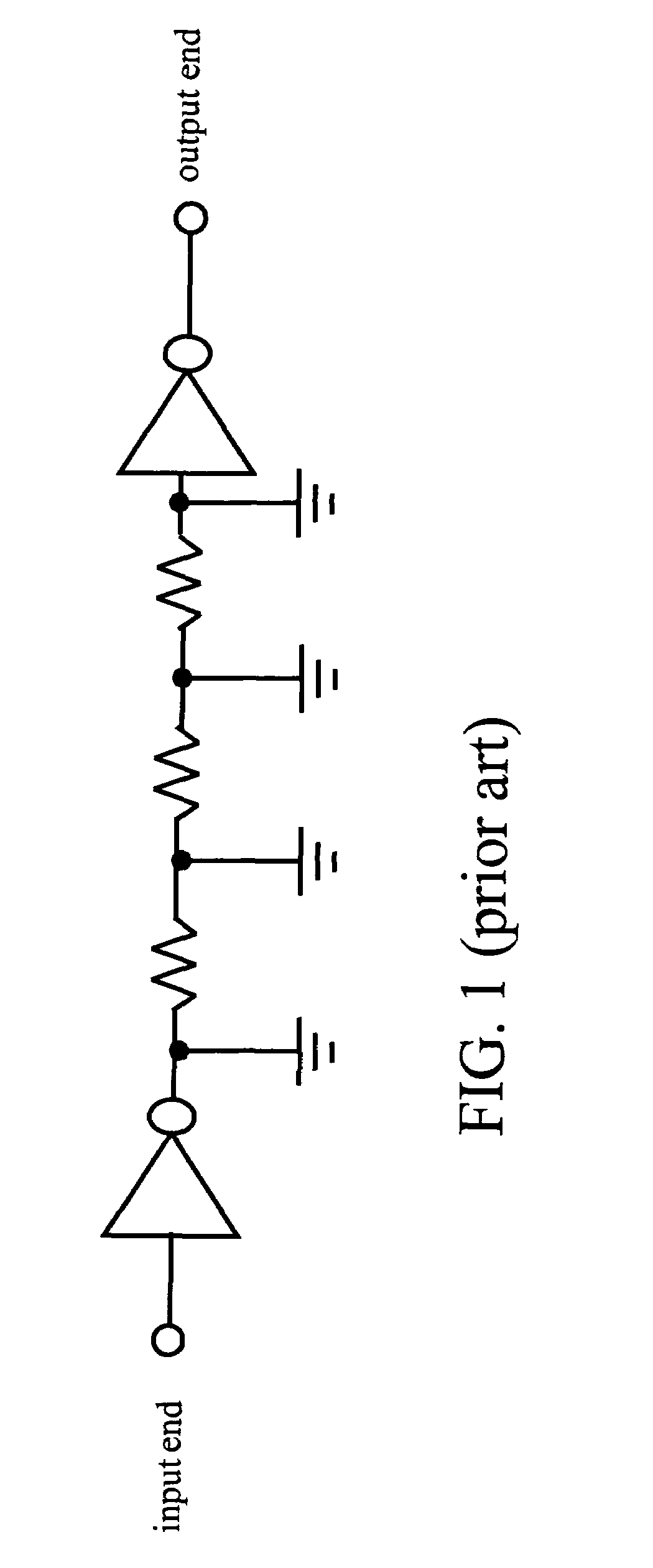
In general, the delay of the logic gate is the major factor that causes time delay.
The progress in the process and the narrowing of the line width of the interconnect cause a greater transmission line delay, thus the delay time of the whole chip is under control of the transmission line delay.
Besides, with the increase of the system clock, the delay caused by the transmission line will be greater than that caused by the logic gate.
Besides, with the reduction of the distance between the line width of the transmission line and the interconnect, the length-width proportion of the cross-section of the transmission line is increased, and the parasitic resistance on the transmission line cannot be avoided.
Moreover, the reduction in the distance between transmission lines may also cause an increase of an adjacent capacitance and a side capacitance.
Then, along with the continuous progress in the process, the area of the chip is reduced, but the package technology of the chip is not improved proportionally.
In circuit operation, the signals on the transmission line must be of full swing; otherwise, transmission errors are likely to happen.
With respect to the power consumption, as the signals are of full swing, the power consumption is large.
Besides, due to the full swing of the signals, great signal delay is caused in the rise delay and fall delay.
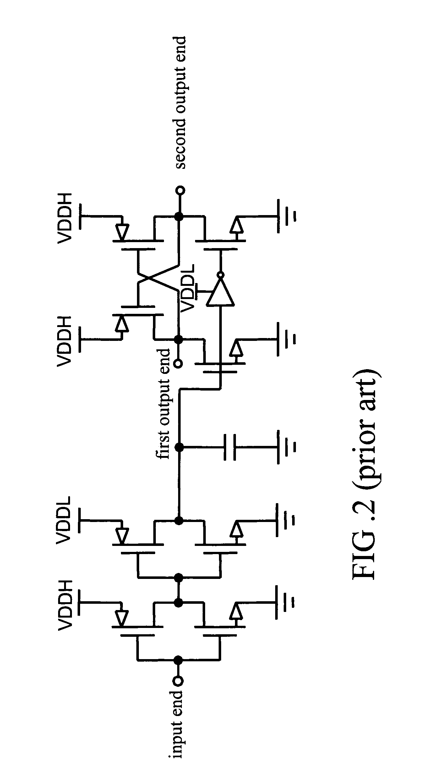
The disadvantage of the circuit architecture is that two supply voltages VDDH, VDDL are required.
When the supply voltage VDDL drops to some extent, the circuit cannot operate normally and the delay of the signal transmission will also be increased accordingly.
As a result, a special process is adopted to achieve the object, resulting in an increase of the cost of the chip.
However, the use of the symmetric source follower driver SSD may limit the swing range on the transmission line.
And as the driving force of the SSD is inadequate, it requires a large-size transistor when pushing a long transmission line.
However, the asymmetric source follower driver ASD may still limit the swing range on the transmission line.
In the circuit architecture, the input end of the receiver is virtually grounded, so the receiving signal is easily interfered by noises, resulting in circuit operating errors.
However, the width of the pulse wave may generate parasitic resistance and parasitic capacitance effects on the transmission line due to various lengths and widths of the transmission line.
However, for the signal transmission on chips, the size of the termination resistor is not so exact due to process drift, thus the design of signal transmission on chips is not suitable.
Referring to FIG. 8, the architecture of a first conventional bidirectional signal circuit is disclosed; wherein double drivers are required to perform signal comparison, thus causing large power consumption.
Besides, as the two drivers require different impedance matches, it is very difficult in practice.
When a direct current (DC) signal is transmitted, a receiving unit will make an offset error.
In the circuit architecture, too many transistor devices are cascaded, so it cannot be applied in a deep sub-micrometer process.
Besides, the design of the circuit architecture can only be adopted when the impedance is known, so it can only be applied to the transmission interface between chips, instead of the transmission in chips.

Method used


Image

  • Bidirectional current-mode transceiver
  • Bidirectional current-mode transceiver
  • Bidirectional current-mode transceiver

Examples


first embodiment

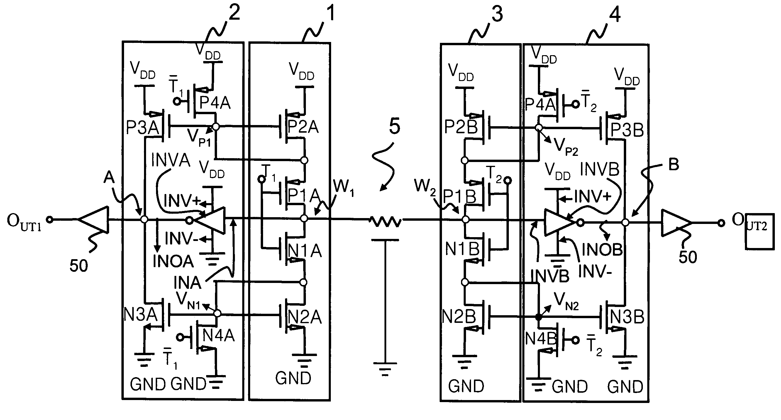
[0062]Referring to FIG. 14, it is a detailed circuit diagram of the bidirectional current-mode transceiver according to the invention. Corresponding to FIG. 13, FIG. 14 depicts detailed circuit diagrams of each of block diagrams of the first and second transmission units 1, 3 correspondingly. As the circuit diagram of the first transmission unit 1 is identical to that of the second transmission unit 3, and the circuit diagram of the first receiving unit 2 is identical to that of the second receiving unit 4, each transistor in the circuit diagrams of the first transmission unit 1 and the second transmission unit 3 in FIG. 14 is given the same name, but distinguished by a different numeral.

[0063]The conversion circuits 10A, 10B in the first and second transmission units 1, 3 include first P-type transistors P1A, P1B and first N-type transistors N1A, N1B, while multiple first current sources 20A, 20B include second P-type transistors P2A, P2B and second N-type transistors N2A, N2B.

[006...

second embodiment

[0129]For the aforementioned several groups of transmission units and receiving units, any group of transmission units can be selectively coupled to a group of receiving units, thereby forming a pair-group bidirectional current-mode transceiver. On the contrary, any group of receiving units can be selectively coupled to a group of transmission units, thereby forming a pair-group bidirectional current-mode transceiver. For example, referring to FIG. 21, it is a circuit diagram according to the invention, wherein the bidirectional current-mode transceiver is constituted by a second group of transmission units and a first group of receiving units.

[0130]In the transmission unit, through changing the connecting mode of the first current sources 20A, 20B, i.e., changing the bias point mode of the first current sources 20A, 20B, the bias point of the first current sources 20A, 20B will not be cascaded with transistors, eliminating limitation to the output current. Therefore, compared with ...

third embodiment

[0131]Referring to FIG. 22, it is a circuit diagram according to the invention, wherein the bidirectional current-mode transceiver is constituted by a third group of transmission units and a first group of receiving units. In the transmission unit, the coupling manner of the conversion circuits 10A, 10B is changed to increase the bias level of the first current sources 20A, 20B, i.e., obtaining a greater driving current, thereby improving the operating speed of the transmission unit. Moreover, the coupling manner of the conversion circuits and the first current sources is applicable under a lower supply voltage VDD.


PUM


Abstract

A bidirectional current-mode transceiver is provided for improving transmission rates on a transmission line in a manner of current signal transmission, and for reducing the swing of the voltage signal on the transmission line by using a termination resistor, thus improving operating speed. Therefore, the provided transceiver can be applied to a long transmission line.

Description

CROSS-REFERENCE TO RELATED APPLICATIONS[0001]This non-provisional application claims priority under 35 U.S.C. § 119(a) on Patent Application No(s). 094143651 filed in Taiwan, R.O.C. on Dec. 9, 2005, the entire contents of which are hereby incorporated by reference.BACKGROUND OF THE INVENTION[0002]1. Field of Invention[0003]The present invention relates to a bidirectional signal transmission circuit device, and more particularly to a bidirectional current-mode transceiver for improving transmission rates on a transmission line in a manner of current signal transmission.[0004]2. Related Art[0005]In the design of a very-large-scale integrated circuit VLSI, the main factors causing time delay are two kinds, in which one case relates to a logic gate causing the time delay and the other relates to a transmission line causing the delay time. In general, the delay of the logic gate is the major factor that causes time delay. However, due to progress in VLSI processes and the trend of system...

Claims


Application Information

Patent Timeline
Patent Type & Authority Patents(United States)
IPC IPC(8): H03K19/0175
CPCH03K19/018592H04L25/0282H04L25/0294H04L25/0298
Inventor HUANG, HONG-YIWU, CHING-CHIEHCHU, YUAN-HUA
Owner IND TECH RES INST
Learn More