Eureka AIR delivers breakthrough ideas for toughest innovation challenges, trusted by R&D personnel around the world.

Precision synthesis of quantum dot nanostructures for fluorescent and optoelectronic devices

a quantum dot nanostructure and fluorescent and optoelectronic device technology, applied in the field of semiconductor nanostructure production methods, can solve the problems of spectral broadening and weakening of photon emission, difficult control of large-scale production of quantum dots having size uniformity, and achieve the effect of enhancing size uniformity

Inactive Publication Date: 2007-12-11
SPIRE
View PDF40 Cites 62 Cited by
  • Summary
  • Abstract
  • Description
  • Claims
  • Application Information

AI Technical Summary

Benefits of technology

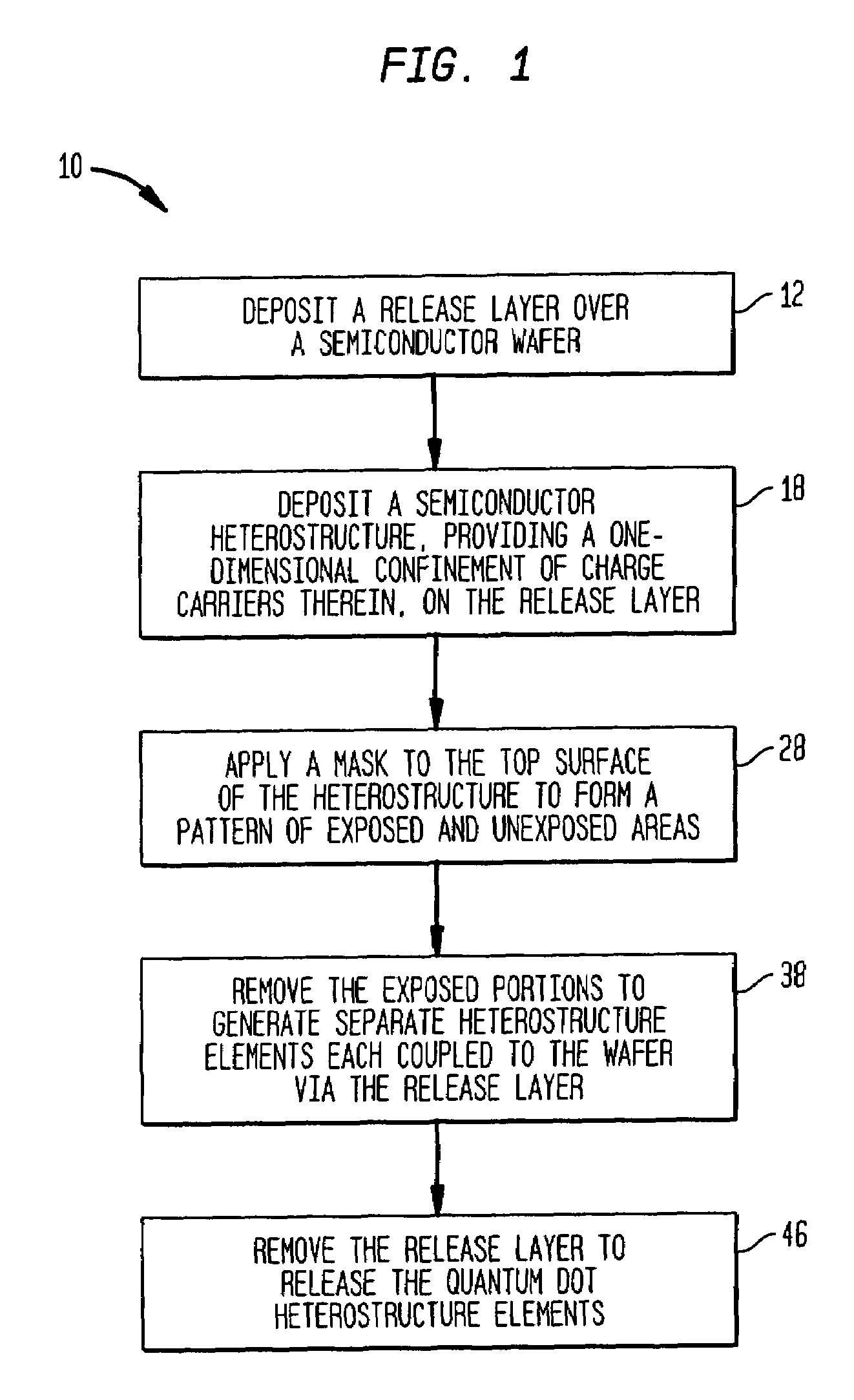
[0007]In one aspect, the present invention provides a method of generating quantum dot structures having enhanced size uniformity by initially depositing a release layer on a semiconductor substrate, e.g., a GaAs substrate, followed by forming a semiconductor heterostructure, which provides a one-dimensional confinement of selected charge carriers therein, on the release layer. A mask can be applied to the surface of the heterostructure to form a pattern of exposed and unexposed portions thereon. The exposed portions are then removed to generate a plurality of separate heterostructure elements, each disposed on a portion of the release layer. As a result of this partial removal process, a highly porous heterostructure remains with the heterostructure layer reduced to an array of individual pillars or columns on the substrate with the release layer separating the heterostructure from the substrate.
[0013]The quantum dot structures generated by utilizing a method according to the teachings of the invention, such as those described above, can be designed to exhibit fluorescence in the visable or infrared (IR) portion of the electromagnetic spectrum, or other desired wavelength bands. Further, the mask utilized in one of the processing steps can be selected such that the sizes of the quantum dot structure vary by less than a few percent. Such size uniformity provides a number of advantages. For example, it allows generating a collection of quantum dot structures that exhibit substantially similar, and preferably identical, emission spectra.

Problems solved by technology

However, despite many recent advances in fabricating quantum dots, large scale production of quantum dots having size uniformity, in a controllable manner, has proven difficult.
Currently available quantum dots typically suffer from size non-uniformities that can result in spectral broadening and weakening of photon emission.

Method used


Image

  • Precision synthesis of quantum dot nanostructures for fluorescent and optoelectronic devices
  • Precision synthesis of quantum dot nanostructures for fluorescent and optoelectronic devices
  • Precision synthesis of quantum dot nanostructures for fluorescent and optoelectronic devices

Examples


Embodiment Construction

[0024]The invention is generally directed to design and synthesis of quantum dot structures, e.g., quantum dot nanoparticles, having improved size uniformity. The terms “nanoparticles,”“nanostructures,” and “quantum dots” are used interchangeably herein to describe materials having dimensions of the order of one or a few nanometers to a few micrometers, more preferably from about 1 to about 100 nanometers of active device structure that possesses optical properties derived from the excitation of a confined population of charge carriers.

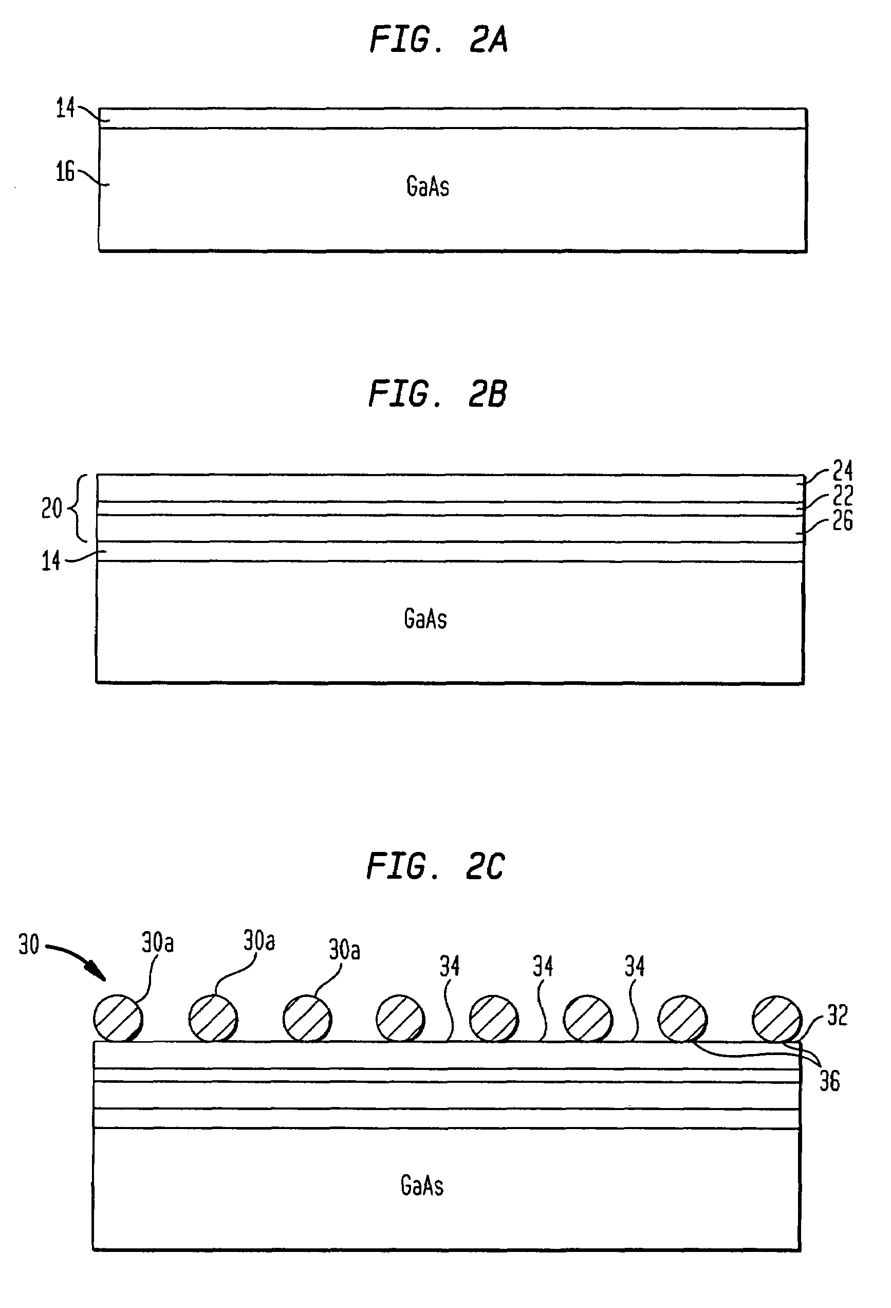
[0025]In general, in a method of the invention for generating quantum dot nanoparticles, a release layer is deposited on a semiconductor wafer followed by deposition of additional layers that form a heterostructure providing a one-dimensional confinement of electrons or other charge carriers. A plurality of ion-blocking nano-particles, e.g., gold particles, are disposed on a top surface of the wafer to form a mask for protecting portions of the hetero...


PUM


Abstract

Methods are disclosed generally directed to design and synthesis of quantum dot nanoparticles having improved uniformity and size. In a preferred embodiment, a release layer is deposited on a semiconductor wafer. A heterostructure is grown on the release layer using epitaxial deposition techniques. The heterostructure has at least one layer of quantum dot material, and optionally, one or more layers of reflective Bragg reflectors. A mask is deposited over a top layer and reactive ion-beam etching applied to define a plurality of heterostructures. The release layer can be dissolved releasing the heterostructures from the wafer. Some exemplary applications of these methods include formation of fluorophore materials and high efficiency photon emitters, such as quantum dot VCSEL devices. Other applications include fabrication of other optoelectronic devices, such as photodetectors.

Description

FIELD OF THE INVENTION[0001]The present invention is directed generally to methods for producing semiconductor nanostructures, and more particularly, to such methods for large scale production of quantum dot particles having enhanced size uniformity.BACKGROUND OF THE INVENTION[0002]Quantum dots are nanometer-sized or micrometer-sized semiconductor structures in which one to a few thousand charge carriers (e.g., electrons) are confined. Such structures are useful in a variety of optical applications because they exhibit narrow spectral emission properties and rapid excited electron decay rates. In device structures, quantum dots possess superior optical properties, in part because they can provide three-dimensional electron confinement.[0003]Quantum dots can be employed in a variety of electronic applications, e.g., to form lasers, LED devices, and photodetectors. Further, the small size of these structures make them particularly useful in assays, diagnostic systems and therapeutic c...

Claims


Application Information

Patent Timeline
Patent Type & Authority Patents(United States)
IPC IPC(8): H01L21/00H01L33/00H01L33/06
CPCB82Y10/00B82Y20/00H01L31/0352H01S5/183H01S5/341H01L33/0079Y10S977/814H01S5/3412H01L33/06H01L33/0093
Inventor LINDEN, KURT J.
Owner SPIRE
Why Eureka
Eureka Blog
Learn More