Semiconductor substrate, semiconductor device, method of manufacturing semiconductor substrate, and method of manufacturing semiconductor device

a semiconductor substrate and semiconductor technology, applied in the direction of crystal growth process, crystal growth process, polycrystalline material growth, etc., can solve the problem of large variation in the thickness of the soi layer, the difficulty of stabilizing the characteristics of the field effect transistor, and the problem of high cost of the soi transistor compared with the field effect transistor formed on bulk semiconductors. achieve the effect of improving the crystal quality of the single crystal semiconductor layer, low cost and low cos

Inactive Publication Date: 2007-11-13
SEIKO EPSON CORP
View PDF6 Cites 3 Cited by
  • Summary
  • Abstract
  • Description
  • Claims
  • Application Information

AI Technical Summary

Benefits of technology

[0009]Therefore, an advantage of the invention is to provide a semiconductor substrate, a semiconductor device, a method of manufacturing a semiconductor substrate, and a method of manufacturing a semiconductor device each capable of forming a single crystal semiconductor layer on an insulating member at low cost while improving the crystal quality of the single crystal semiconductor layer.
[0010]In order for obtaining the advantage described above, a semiconductor substrate according to an aspect of the invention includes a single-crystallized semiconductor layer single-crystallized while being supported above a single crystal semiconductor substrate via a seed crystal and an embedded insulating layer embedded between the single-crystallized semiconductor layer and the single crystal semiconductor substrate.
[0011]Thus, the single-crystallized semiconductor layer can be formed by the thermal treatment on the non-crystalline semiconductor layer via the seed crystal while the non-crystalline semiconductor layer is held above the single crystal semiconductor substrate so that the non-crystalline semiconductor layer does not have contact with the oxide film. Therefore, the lateral single crystallization of the non-crystalline semiconductor layer can be prevented from being constricted by the oxide film, thus the single-crystallized semiconductor layer can be formed on the insulating member at low cost while improving the crystal quality of the single-crystallized semiconductor layer, and further a large sized single-crystallized semiconductor layer can be obtained.
[0012]Further, a semiconductor device according to another aspect of the invention includes a single-crystallized semiconductor layer single-crystallized while being held above the single crystal semiconductor substrate via a seed crystal, an embedded insulating layer embedded between the single-crystallized semiconductor layer and the single crystal semiconductor substrate, a gate electrode disposed on at least one of the single-crystallized semiconductor layer and a side wall of the single-crystallized semiconductor layer, a source layer formed in the single-crystallized semiconductor layer and disposed on one side of the gate electrode, a drain layer formed in the single-crystallized semiconductor layer and disposed on the other side of the gate electrode.
[0013]Accordingly, the single crystallization of the non-crystalline semiconductor layer can be proceeded while preventing the lateral single crystallization of the non-crystalline semiconductor layer from being constricted by the oxide film, thus the single-crystallized semiconductor layer can be formed on the insulating member at low cost while improving the crystal quality of the single-crystallized semiconductor layer, and further a large sized single-crystallized semiconductor layer can be obtained.
[0014]Further, a method of manufacturing a semiconductor substrate according to another aspect of the invention includes the step of forming an insulating layer on a single crystal semiconductor substrate, the step of forming a non-crystalline semiconductor layer on the insulating layer, the step of forming an insulating film on the non-crystalline semiconductor layer, the step of forming an opening section for exposing a part of a surface of the single crystal semiconductor substrate through the insulating film, the non-crystalline semiconductor layer and the insulating layer, the step of forming a single crystal semiconductor layer embedded in the opening section so as to have contact with the non-crystalline semiconductor layer, the step of removing the insulating film and the insulating layer while the single crystal semiconductor layer supporting the non-crystalline semiconductor layer above the single crystal semiconductor substrate, the step of forming a single-crystallized semiconductor layer obtained by single-crystallizing the non-crystalline semiconductor layer using the single crystal semiconductor layer as a seed by providing a thermal treatment on the non-crystalline semiconductor layer from which the insulating film and the insulating layer are removed, and the step of filling a gap between the single-crystallized semiconductor layer and the single crystal semiconductor substrate with an embedded insulating layer.

Problems solved by technology

Therefore, the SOI transistors problematically incur higher cost in comparison with field effect transistors formed on bulk semiconductors.
Further, the ion-implantation process or the polishing process causes large variation in the thickness of the SOI layer.
Therefore, if the SOI layer is made thinner for forming the complete depletion type of SOI transistor, it is problematically difficult to stabilize the characteristics of the field effect transistor.
Accordingly, the lateral single crystallization of the amorphous silicon layer is constricted by the oxide film to cause degradation of crystal quality of the single crystal semiconductor layer, and also it is problematically difficult to obtain a large sized single crystal semiconductor layer.

Method used


Image

  • Semiconductor substrate, semiconductor device, method of manufacturing semiconductor substrate, and method of manufacturing semiconductor device
  • Semiconductor substrate, semiconductor device, method of manufacturing semiconductor substrate, and method of manufacturing semiconductor device
  • Semiconductor substrate, semiconductor device, method of manufacturing semiconductor substrate, and method of manufacturing semiconductor device

Examples


first embodiment

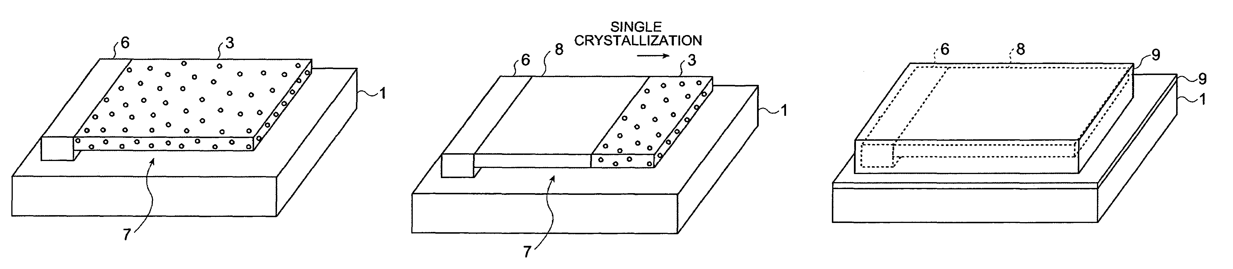
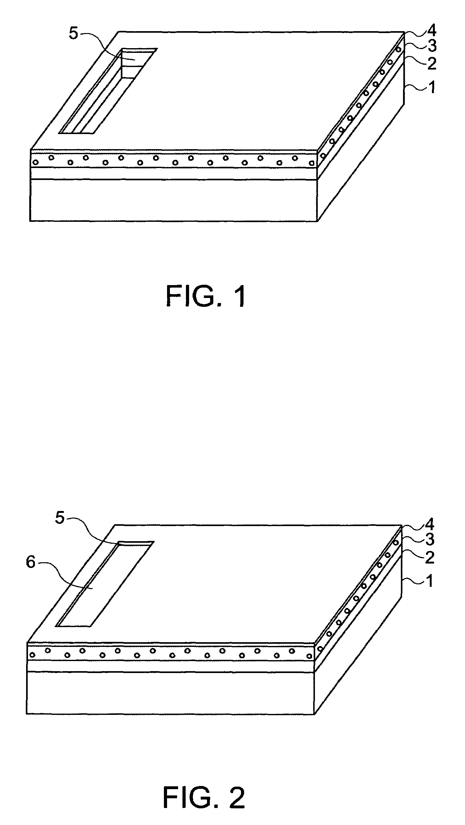
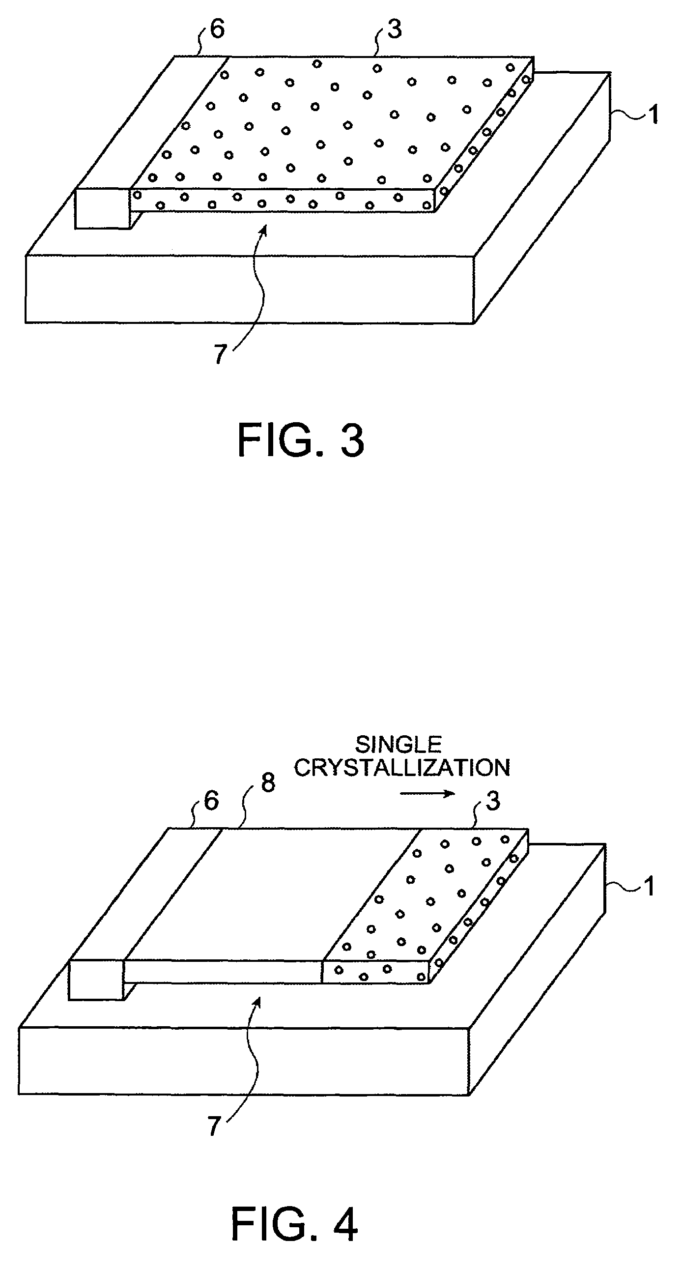
[0049]FIGS. 1 through 8 are perspective views showing the method of manufacturing a semiconductor device according to the invention.

[0050]In FIG. 1, a silicon oxide film 2, a non-crystalline semiconductor layer 3, and a silicon oxide film 4 are sequentially formed on a single crystal semiconductor substrate 1 by a CVD process or the like. And then, by patterning the silicon oxide film 2, the non-crystalline semiconductor layer 3, and the silicon oxide film 4 using a photolithography technology and an etching technology, an opening section 5 for exposing a part of the surface of the single crystal semiconductor substrate 1 through the silicon oxide film 2, the non-crystalline semiconductor layer 3 and the silicon oxide film 4 is formed. Note that as a material for the single crystal semiconductor substrate 1 and the non-crystalline semiconductor layer 3, for example, Si, Ge, SiGe, SiC, SiSn, PbS, GaAs, InP, GaP, GaN, ZnSe or the like can be used. Further, in order for exposing a part...

second embodiment

[0069]FIGS. 9 through 12 are perspective views showing the method of manufacturing a semiconductor device according to the invention. In FIG. 9, a silicon oxide film 22 is formed on a single crystal semiconductor substrate 21 by a CVD method or the like. And then, an opening section 25 for exposing a part of a surface of the single crystal semiconductor substrate 21 through the silicon oxide film 22 is formed by patterning the silicon oxide film 22 using a photolithography technology and an etching technology.

[0070]Subsequently, as shown in FIG. 10, a non-crystalline semiconductor layer 23 disposed so as to have contact with the single crystal semiconductor substrate 21 via the opening section 25 is formed on the silicon oxide film 22 by a CVD method or the like. Note that an amorphous semiconductor layer can be used as the non-crystalline semiconductor layer 23.

[0071]Subsequently, as shown in FIG. 11, a part of the silicon oxide film 22 disposed under the non-crystalline semiconduc...

third embodiment

[0076]FIGS. 13 through 18 are perspective views showing the method of manufacturing a semiconductor device according to the invention.

[0077]In FIG. 13, a silicon oxide film 32 is formed on a single crystal semiconductor substrate 31 by a CVD method or the like. And then, an opening section 35 for exposing a part of a surface of the single crystal semiconductor substrate 31 through the silicon oxide film 32 is formed by patterning the silicon oxide film 32 using a photolithography technology and an etching technology.

[0078]Subsequently, as shown in FIG. 14, an non-crystalline semiconductor layer 33 disposed so as to have contact with the single crystal semiconductor substrate 31 via the opening section 35 is formed on the silicon oxide film 32 by a CVD method or the like. Note that an amorphous semiconductor layer can be used as the non-crystalline semiconductor layer 33. And then, side walls of the non-crystalline semiconductor layer 33 are exposed by patterning the non-crystalline ...


PUM


Abstract

A method of manufacturing a semiconductor device, includes: forming an insulating layer on a single crystal semiconductor substrate; forming a non-crystalline semiconductor layer on the insulating layer; forming an insulating film on the non-crystalline semiconductor layer; forming an opening section for exposing a part of a surface of the single crystal semiconductor substrate through the insulating film, the non-crystalline semiconductor layer and the insulating layer; forming a single crystal semiconductor layer embedded in the opening section so as to have contact with the non-crystalline semiconductor layer; removing the insulating film and the insulating layer while the single crystal semiconductor layer supporting the non-crystalline semiconductor layer above the single crystal semiconductor substrate; forming a single-crystallized semiconductor layer obtained by single-crystallizing the non-crystalline semiconductor layer using the single crystal semiconductor layer as a seed by providing a thermal treatment on the non-crystalline semiconductor layer from which the insulating film and the insulating layer are removed; filling a gap between the single-crystallized semiconductor layer and the single crystal semiconductor substrate with an embedded insulating layer; forming a gate electrode on the single-crystallized semiconductor layer; and forming in the single-crystallized semiconductor layer a source layer disposed on one side of the gate electrode and a drain layer disposed on the other side of the gate electrode.

Description

BACKGROUND OF THE INVENTION[0001]1. Technical Field[0002]The invention relates to a semiconductor substrate, a semiconductor device, a method of manufacturing a semiconductor substrate, and a method of manufacturing a semiconductor device, and is particularly suitable for application to a field effect transistor formed on an SOI (Silicon On Insulator) substrate.[0003]2. Related Art[0004]A field effect transistor formed on an SOI substrate has availability drawing attention in view of its easiness in element separation, latch-up free, small source-drain junction capacitance. In particular, since a complete depletion type SOI transistor can offer low power consumption and high operation speed and is easy to be driven with a low voltage, researches for making the SOI transistor in the complete depletion mode are actively conducted. Here, as the SOI substrate, for example, an SIMOX (Separation by Implanted Oxygen) substrate or a laminated substrate is used as disclosed in JP-A-2002-2995...

Claims


Application Information

Patent Timeline
Patent Type & Authority Patents(United States)
IPC IPC(8): H01L21/00H01L21/84
CPCH01L21/2022H01L29/785H01L29/66795H01L21/02389H01L21/02667H01L21/02543H01L21/02488H01L21/02535H01L21/02568H01L21/02642H01L21/02395H01L21/02529H01L21/02392H01L21/02384H01L21/02409H01L21/02645H01L21/02532H01L21/02598H01L21/0254H01L21/0256H01L21/02546H01L21/02378H01L21/02381H01L21/02417H01L21/02639
Inventor KANEMOTO, KEI
Owner SEIKO EPSON CORP
Why Eureka
Try Eureka