
Semiconductor apparatus for white light generation and amplification

a technology of white light generation and amplification, applied in the field of semiconductor devices, can solve the problems of poor optoelectronic conversion efficiency, high cost, critical disadvantage, etc., and achieve the effect of generating white light with high power, reducing packaging cost, and greatly improving optoelectronic conversion efficiency

Active Publication Date: 2007-09-18
NAT CENT UNIV
View PDF1 Cites 3 Cited by
  • Summary
  • Abstract
  • Description
  • Claims
  • Application Information

AI Technical Summary

Benefits of technology

This approach enhances optoelectronic conversion efficiency, reduces heat loss, and achieves stable, uniform white light generation across varying current biases, applicable to white-light generators and amplifiers in optical fiber communication systems.

Problems solved by technology

But, the first prior art has the following disadvantages:1. Because the red light and the yellow light generated by a semiconductor of the white-light generator and amplifier according to the first prior art are excited by the blue light except directly electronically excited, the efficiency of the optoelectronic conversion is quite poor.2. Because the wavelength of the (blue) light for exciting is far from the wavelengths of the (red and yellow) lights to be exited, extra heat loss will happen on operating the element while shortening its operation life.3. The packaging of the semiconductor of the white-light generator and amplifier according to the first prior art requires doping with fluorescent powder so its cost become higher.
Yet, such a LED is not widely accepted by the market for it still has a critical disadvantage.
Because the movement of holes is far slower than that of electrons, the quantum wells which generate light are gathered up near p-side so that the efficiency of light emission for the quantum wells that generate light of the other colors will become very poor.

Method used


Image

  • Semiconductor apparatus for white light generation and amplification
  • Semiconductor apparatus for white light generation and amplification
  • Semiconductor apparatus for white light generation and amplification

Examples


Embodiment Construction

)

[0015]The following descriptions of the preferred embodiments are provided to understand the features and the structures of the present invention.

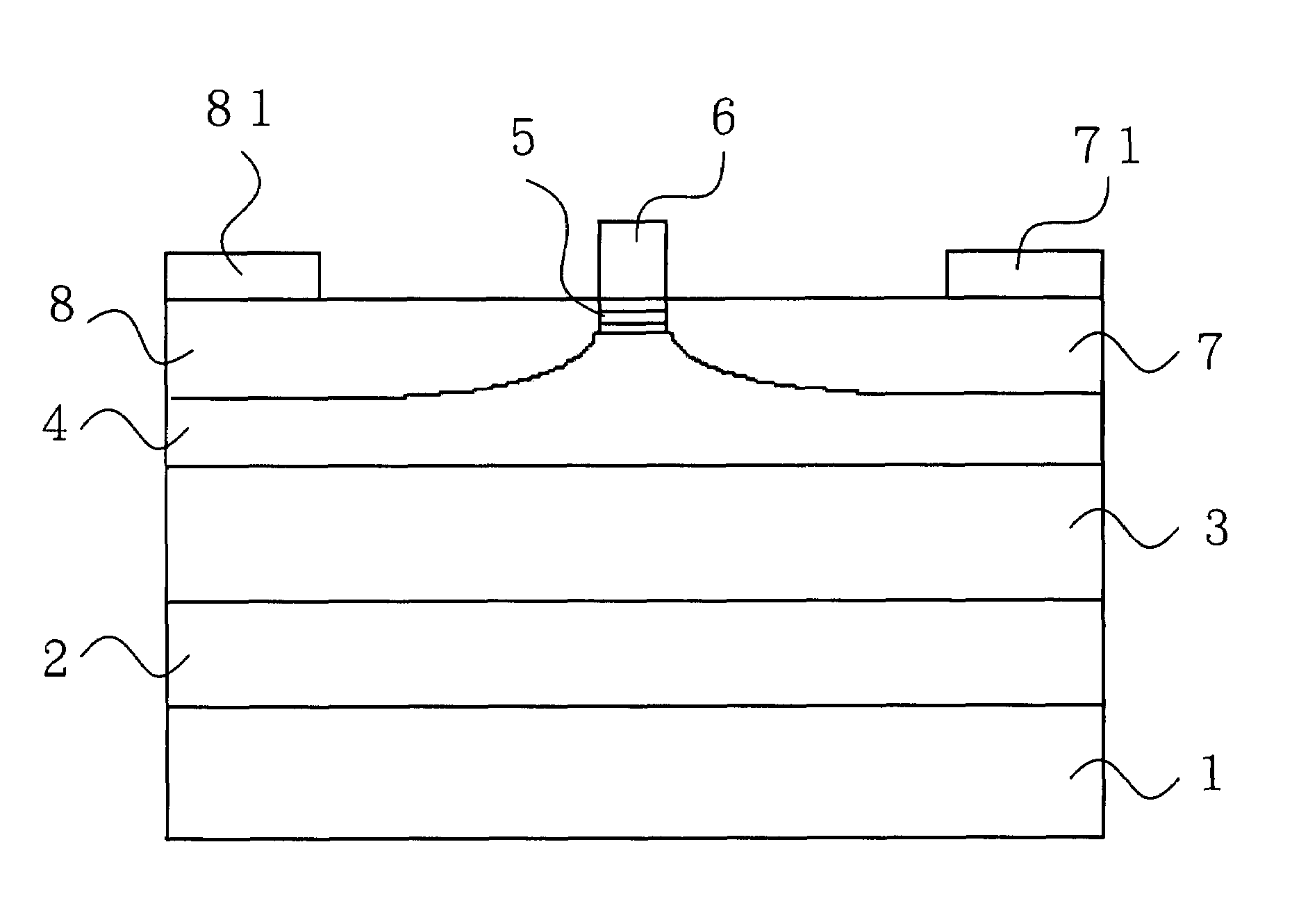
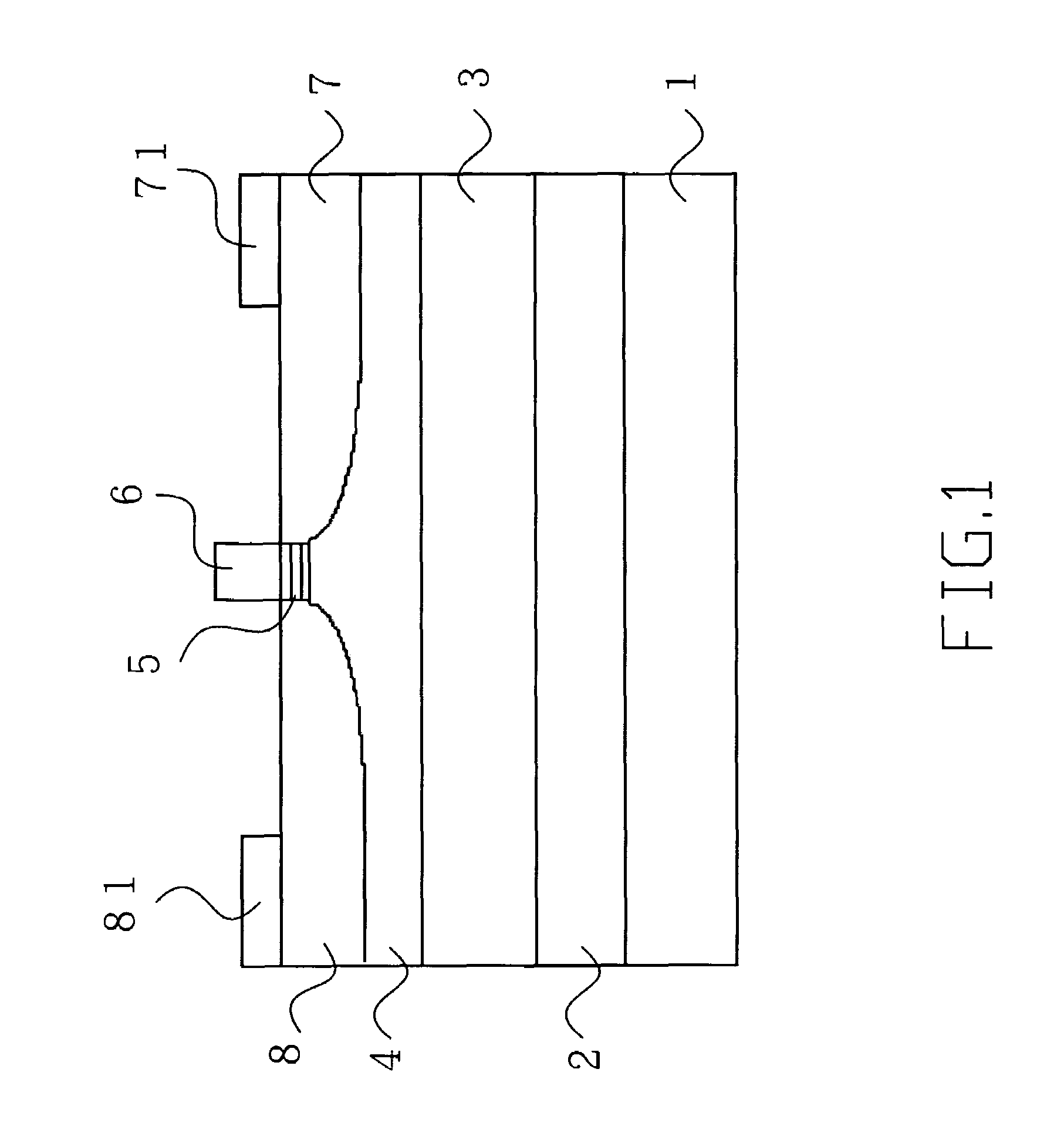
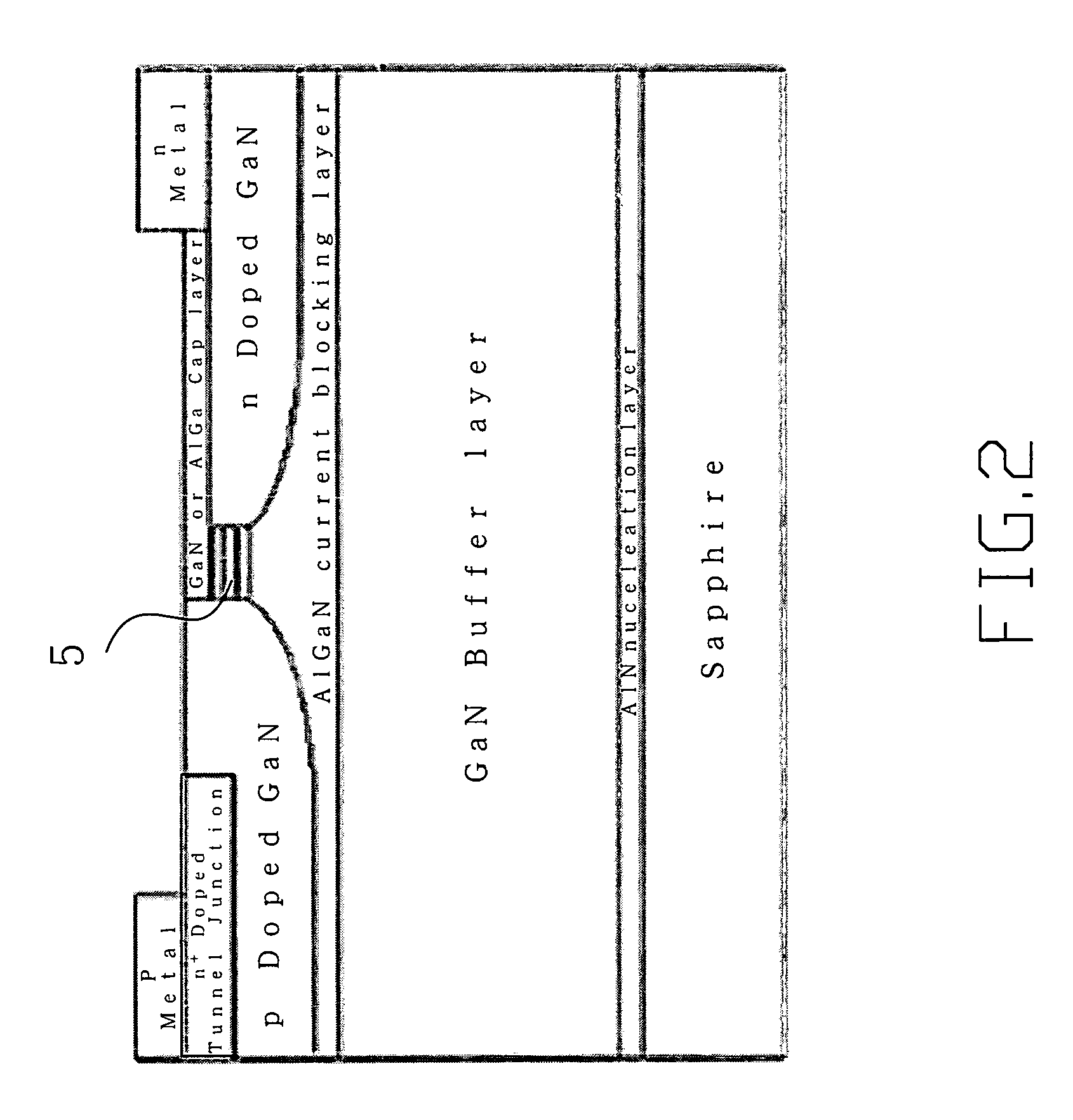
[0016]Please refer to FIG.1 and FIG.2, which are a structural view according the present invention and a structural view according a preferred embodiment of the present invention. As shown in the figures, the present invention comprises a base substrate 1; a first optical cladding 2 formed on the base substrate 1; a second optical cladding 3 formed on the first optical cladding 2; a current blocking and optical cladding layer 4 formed on the second optical cladding 3; a multi-wavelength quantum well (MQW) 5 formed on the current blocking optical cladding layer 4; and a wide-bandgap optical cladding 6 formed on the MQW 5, so that a semiconductor apparatus for white light generation and amplification is constructed. Therein, the base substrate 1 can be made of any kind of compound semiconductor, such as GaAs, InP, AlN or GaN; or an insulato...


PUM


Abstract

The present invention is a semiconductor apparatus for white light generation and amplification, where, under different current bias, white light can be generated steadily and evenly by folding up multi-wavelength quantum wells and by side-injecting a current. And, the white light can be excited out electronically without mingling with a fluorescent powder so that the cost for sealing is reduced. Because the light is directly excited out by electricity to prevent from energy loss during fluorescence transformation, the light generation efficiency of the present invention is far greater than that of the traditional phosphorus mingled with light-emitting diode of white light. Besides, concerning the characteristics of the white light, the spectrum of the white light can be achieved by adjusting the structure and / or the number of the quantum wells while preventing from being limited by the atomic emission lines of the fluorescent powder.

Description

FIELD OF THE INVENTION[0001]The present invention relates to a semiconductor apparatus; more particularly, relates to, by stacking MQWs (multi-wavelength quantum wells) and injecting a current from the sidewall of MQW, the present invention can be applied to white-light generator and a white-light amplifier in an optical fiber communication.DESCRIPTION OF THE RELATED ARTS[0002]Please refer to FIG. 3 and FIG. 4, which, according to the first prior art, are a structural view and a view showing the spectrum of the electronically-excited light. The first prior art uses a blue LED (Light Emitting Diode) to excite the red fluorescent powder and the yellow one. But, the first prior art has the following disadvantages:[0003]1. Because the red light and the yellow light generated by a semiconductor of the white-light generator and amplifier according to the first prior art are excited by the blue light except directly electronically excited, the efficiency of the optoelectronic conversion is...

Claims


Application Information

Patent Timeline
Patent Type & Authority Patents(United States)
IPC IPC(8): H01L27/15H01L31/12H01L31/153H01L33/00H01L33/08H01L33/32
CPCB82Y20/00H01L33/08H01S5/227H01L33/32H01S5/0424H01S5/2206H01S5/3095H01S5/34333
Inventor SHI, JIN-WEISHEU, JINN-KONG
Owner NAT CENT UNIV
Learn More