Image display device
a display device and image technology, applied in the direction of identification means, instruments, static indicating devices, etc., can solve the problems of forming a wiring layer, affecting the appearance of the liquid crystal display panel, and the connection failure between the semiconductor device and the wiring layer mounted on the liquid crystal display devi
- Summary
- Abstract
- Description
- Claims
- Application Information
AI Technical Summary
Benefits of technology
Problems solved by technology
Method used
Image

Examples
embodiment 1
[Module of Liquid Crystal Display Device]
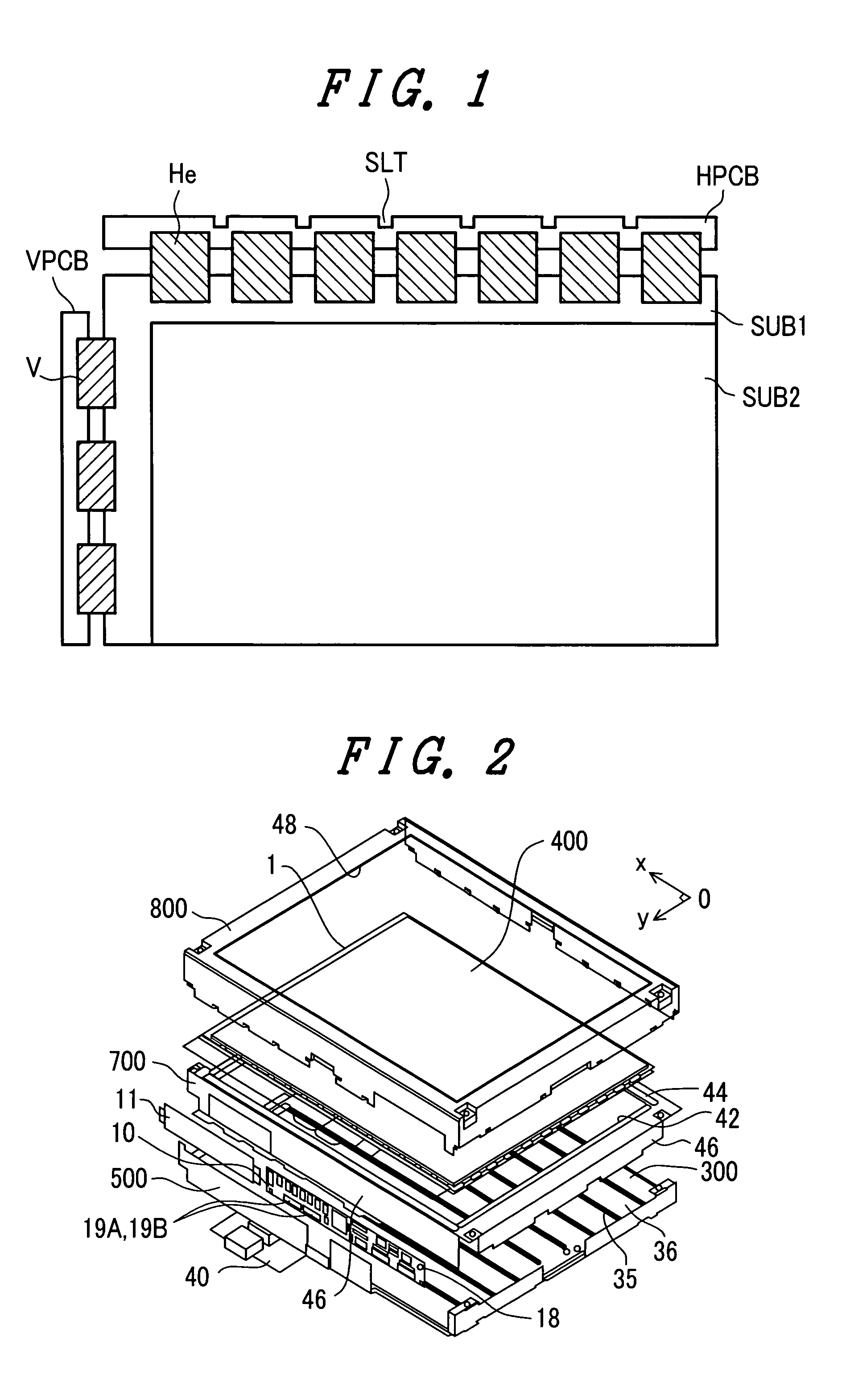
[0043]FIG. 2 is an exploded perspective view showing one embodiment of a module of a liquid crystal display device according to the present invention.
[0044]The liquid crystal display device shown in the drawing is roughly constituted of a liquid crystal display panel module 400, a backlight 300, a resin frame body 500, an intermediate frame 700, an upper frame 800 and the like, which are formed into a module.
[0045]Here, in this embodiment, a reflector which constitutes a portion of the backlight 300 is formed on a bottom surface of the resin frame body 500. Although the physical distinction between the resin frame body 500 and the backlight 300 is difficult, they can be functionally distinguished from each other in the above-mentioned manner.
[0046]Hereinafter, respective members which form the liquid crystal display device will be sequentially explained.
[Liquid Crystal Display Panel Module 400]
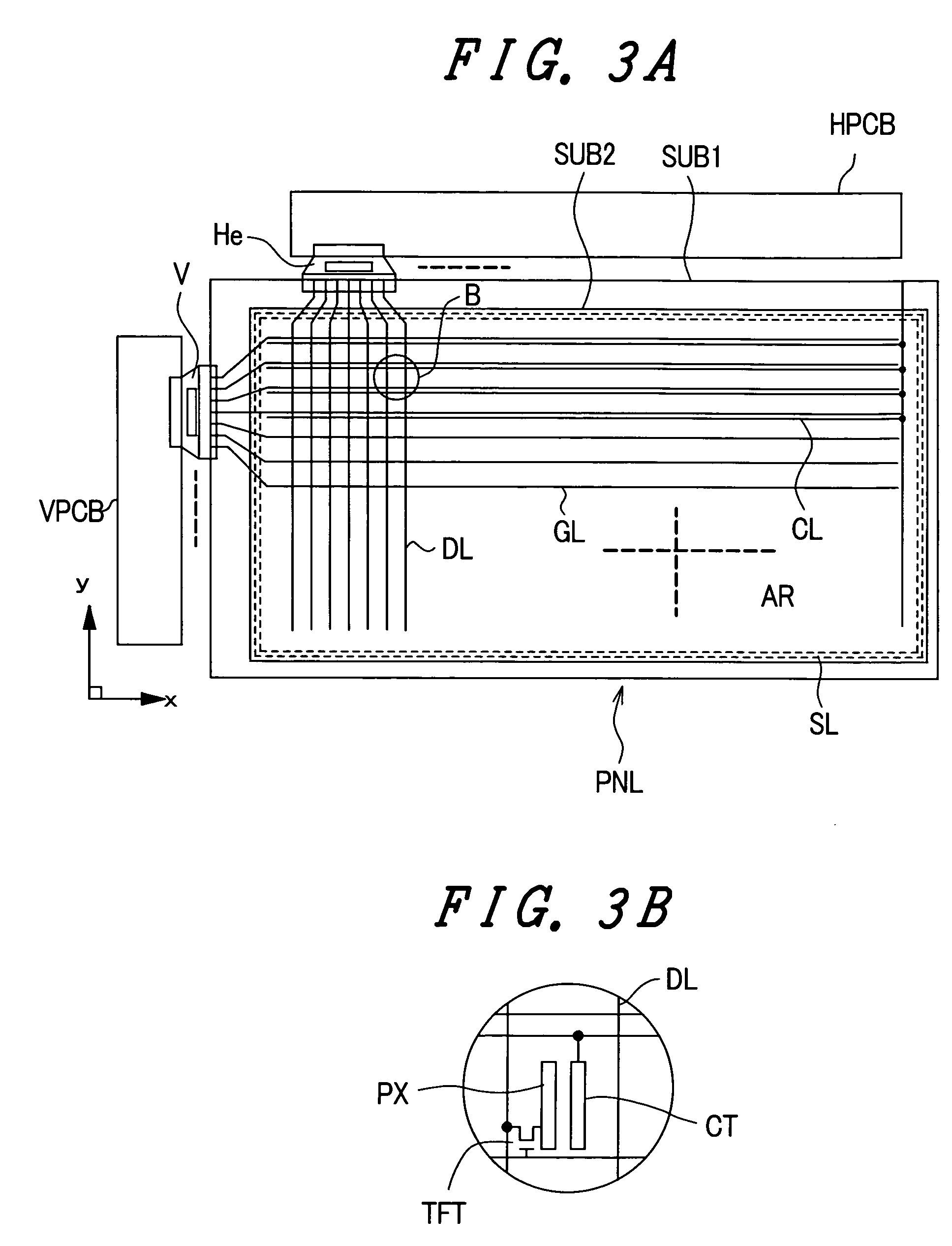
[0047]The liquid crystal display panel module 400...
embodiment 2
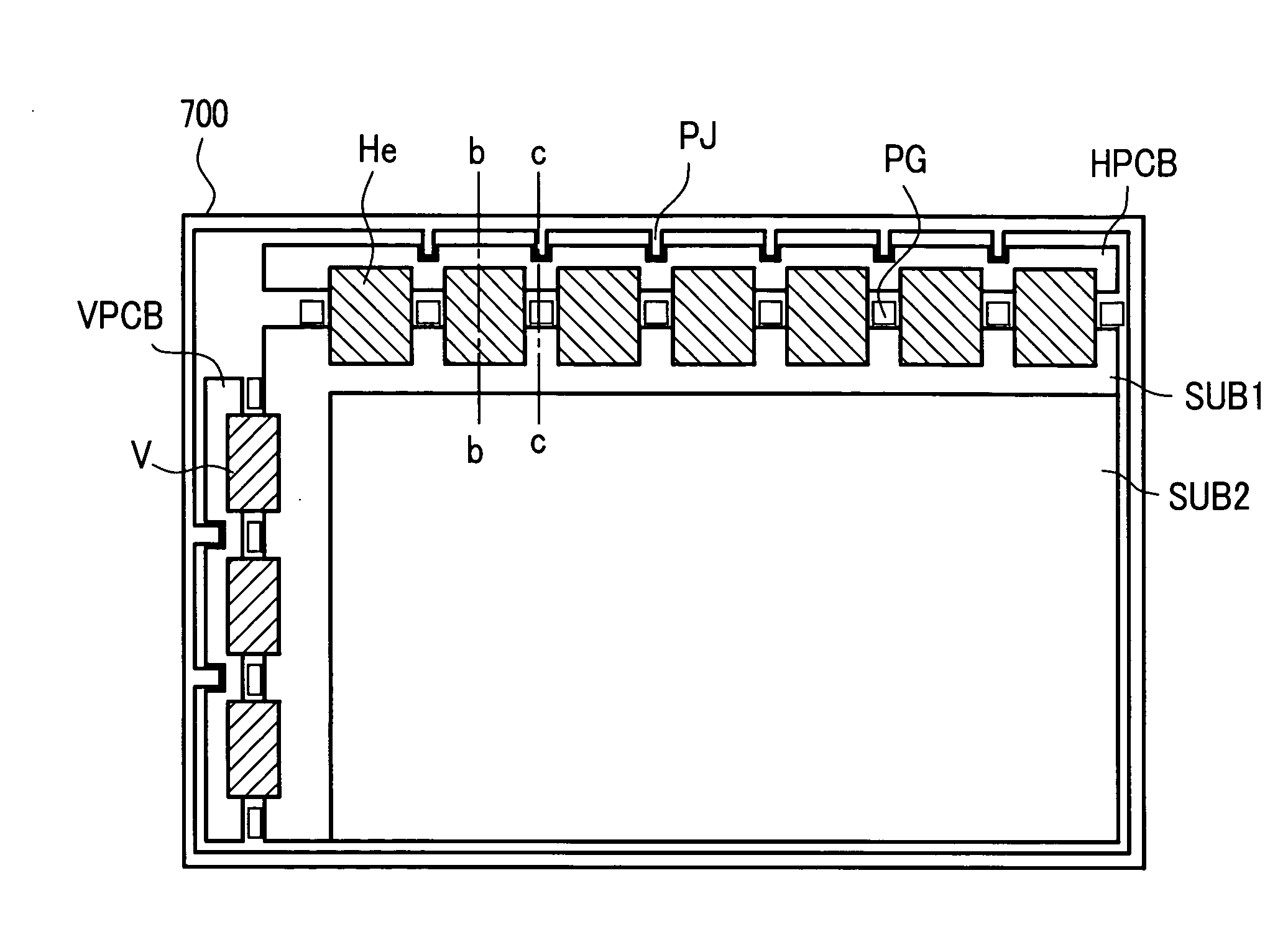
[0079]FIG. 4 is a plan view showing another embodiment of the liquid crystal display device according to the present invention, which generally corresponds to that of FIG. 1.
[0080]The feature which makes this embodiment different from the embodiment 1 shown in FIG. 1 lies in the fact that slits SLT similar to the slits formed in the above-mentioned video signal driving printed circuit board HPCB are also formed in the scanning signal driving printed circuit board VPCB.
[0081]Since stress and strain generated on the video signal driving printed circuit board of this kind is increased in proportion to the length thereof, it is more effective to mount the slits SLT in the video signal driving printed circuit board HPCB than in the scanning signal driving printed circuit board VPCB. However, due to the recent trend toward increasing the size of the liquid crystal display panel PNL, the length of the scanning signal driving printed circuit board VPCB is also elongated, and, hence, it is n...
embodiment 3
[0082]FIGS. 5A and 5B are diagrams showing examples of the shape of the slits formed in the video signal driving printed circuit board HPCB or in the scanning signal driving printed circuit board VPCB.
[0083]First of all, in FIG. 5A, the notch formed on the signal driving printed circuit board has a rectangular shape and the depth thereof is not less than 1 mm and not more than 5 mm. The reason for setting the depth of the notch to not less than 1 mm is that the desired stress relaxation is not obtained when the depth of the notch is less than 1 mm. Further, the reason for setting the depth of the notch to not more than 5 mm is that, when the depth of the notch exceeds 5 mm, the width of the signal driving printed circuit board becomes excessively narrow at the slit SLT portion, and, hence, a so-called torsional stress is easily generated at the signal driving printed circuit board, whereby the stress applied to the signal driving circuit is increased to the contrary.
[0084]Further, i...
PUM
| Property | Measurement | Unit |
|---|---|---|
| depth | aaaaa | aaaaa |
| depth | aaaaa | aaaaa |
| width | aaaaa | aaaaa |
Abstract
Description
Claims
Application Information
 - R&D
- Intellectual Property
- Life Sciences
- Materials
- Tech Scout
- Unparalleled Data Quality
- Higher Quality Content
- 60% Fewer Hallucinations
Browse by: Latest US Patents, China's latest patents, Technical Efficacy Thesaurus, Application Domain, Technology Topic, Popular Technical Reports.
© 2025 PatSnap. All rights reserved.Legal|Privacy policy|Modern Slavery Act Transparency Statement|Sitemap|About US| Contact US: help@patsnap.com