Plasma processing apparatus
a processing apparatus and plasma technology, applied in the field of plasma processing apparatus, can solve the problems of unsatisfactory plasma density distribution of related-art apparatus
- Summary
- Abstract
- Description
- Claims
- Application Information
AI Technical Summary
Benefits of technology
Problems solved by technology
Method used
Image
Examples
first embodiment
(First Embodiment)
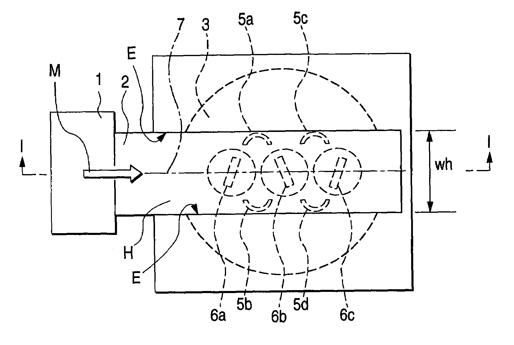
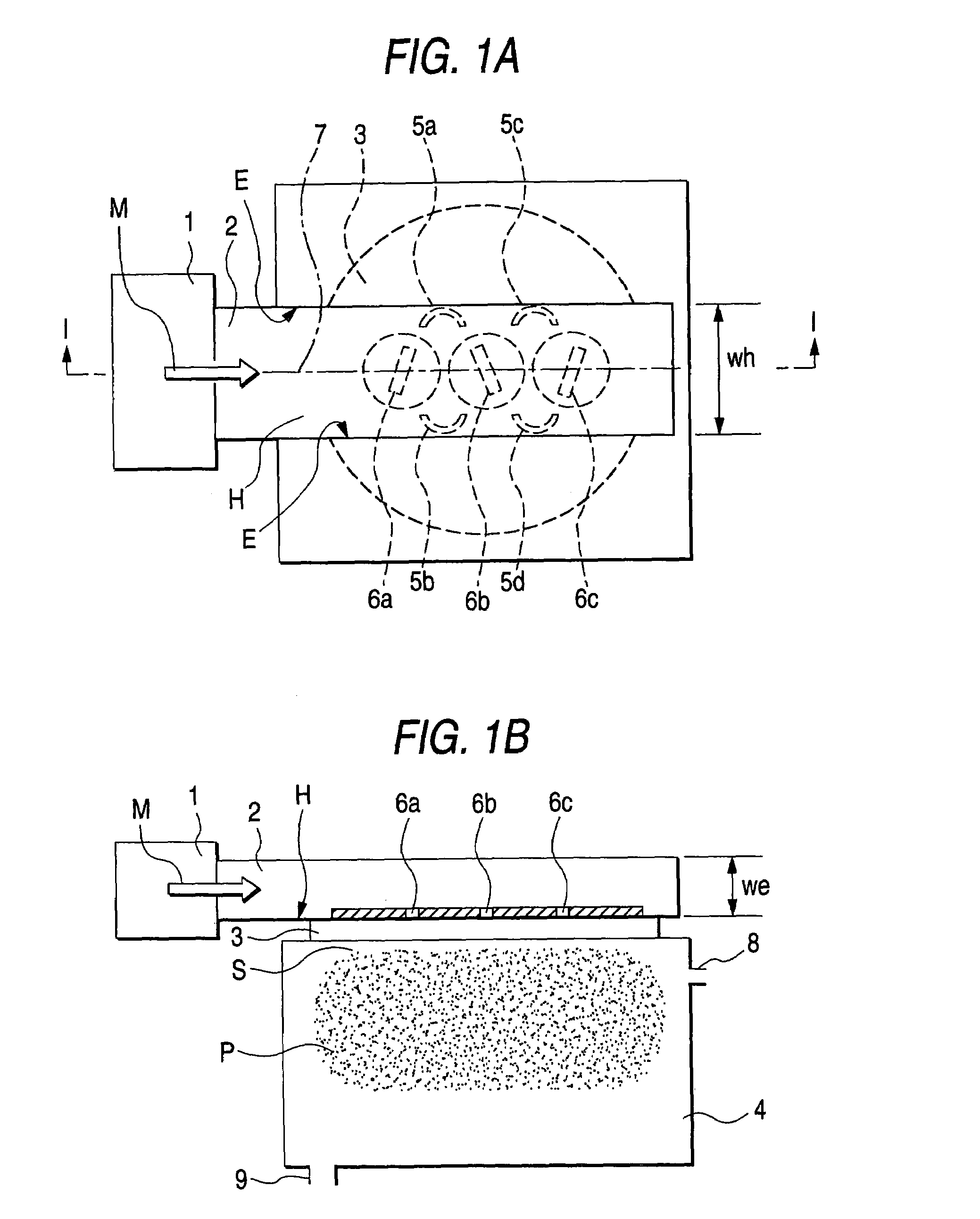
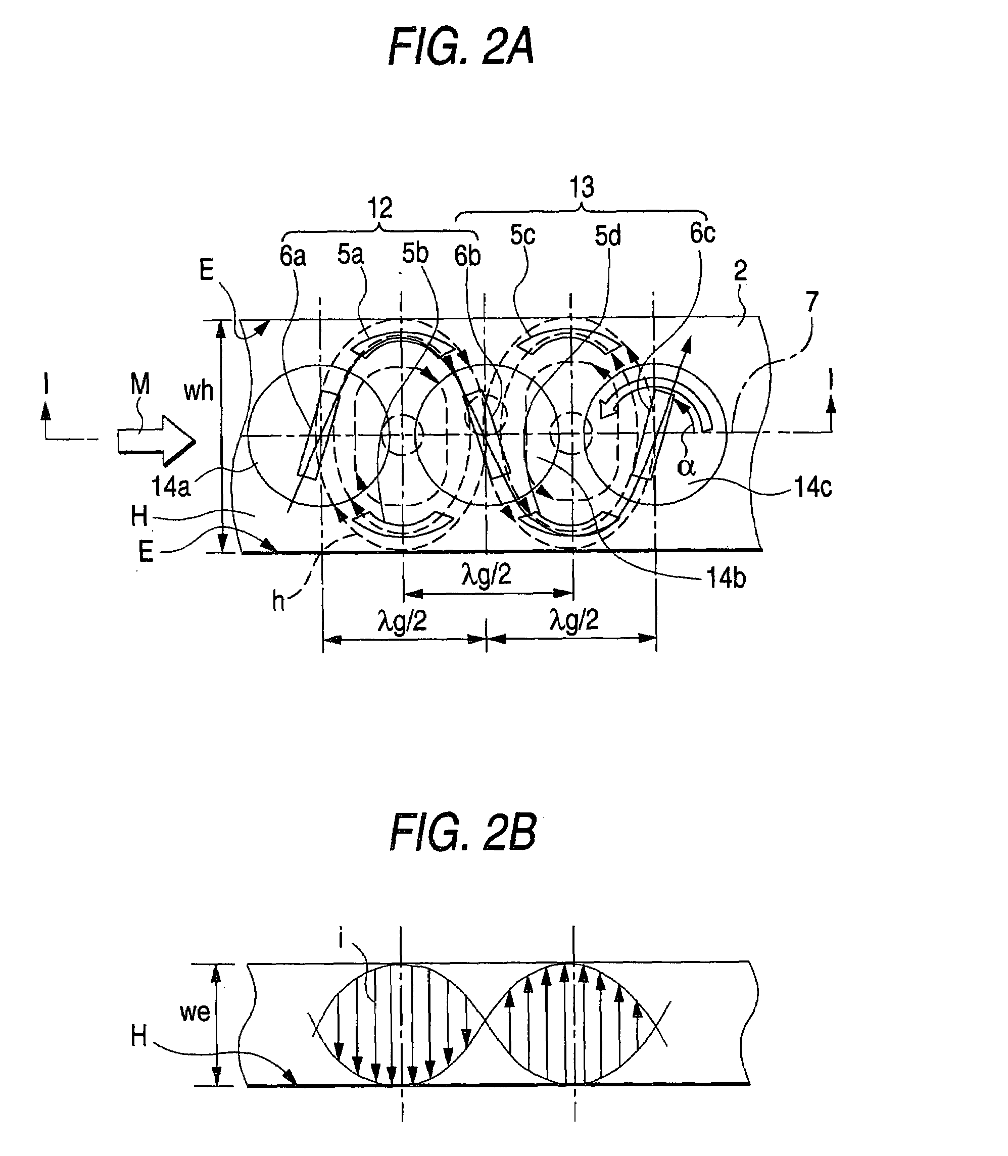
[0024]FIGS. 1A and 1B are schematic configuration views typically showing the whole of a plasma processing apparatus according to a first embodiment of the invention. FIG. 1A is a top view, and FIG. 1B is a sectional view taken on line I—I in FIG. 1A. FIGS. 2A and 2B are schematic diagrams showing shapes of apertures and layouts of slot antennas and the electromagnetic field distribution in a microwave waveguide in the plasma processing apparatus according to the first embodiment of the invention. FIG. 2A is a top view, andFIG. 2B is a sectional view taken on line I—I in FIG. 2A. FIG. 3 is a partial top view showing the state where microwave energy is transmitted in the plasma processing apparatus according to the first embodiment of the invention.
[0025]The plasma processing apparatus shown in FIGS. 1A and 1B has a microwave output portion 1, a microwave waveguide 2, a dielectric window 3 and a chamber 4. The microwave output portion 1 has a high-voltage power supp...
second embodiment
(Second Embodiment)
[0048]FIG. 7 is a schematic configuration view typically showing the whole of a plasma processing apparatus according to a second embodiment of the invention. The plasma processing apparatus according to this embodiment is adapted so that the electric-field-direction distance e of the microwave waveguide 2 varies continuously in the direction in which the microwaves M are transmitted. When the electric-field-direction distance e is varied, the excited state of plasma varies so that the plasma density can be equalized.
[0049]In order to vary the electric-field-direction distance e in the microwave waveguide 2, an adjustment member (flap plate) 22 is attached to a surface of the microwave waveguide 2 opposite to the magnetic field side H, that is, a top surface 21 of the microwave waveguide 2 as shown in FIG. 7. The flap plate 22 is machined out of a nonmagnetic conductive material such as an aluminum alloy, and attached to the top surface 21 at two places through ad...
PUM
| Property | Measurement | Unit |
|---|---|---|
| frequency | aaaaa | aaaaa |
| pressure | aaaaa | aaaaa |
| width | aaaaa | aaaaa |
Abstract
Description
Claims
Application Information
 - R&D
- Intellectual Property
- Life Sciences
- Materials
- Tech Scout
- Unparalleled Data Quality
- Higher Quality Content
- 60% Fewer Hallucinations
Browse by: Latest US Patents, China's latest patents, Technical Efficacy Thesaurus, Application Domain, Technology Topic, Popular Technical Reports.
© 2025 PatSnap. All rights reserved.Legal|Privacy policy|Modern Slavery Act Transparency Statement|Sitemap|About US| Contact US: help@patsnap.com


