
Method of post-deposition treatment for silicon oxide film

a technology of silicon oxide film and post-deposition treatment, which is applied in the direction of chemical vapor deposition coating, coating, electric discharge tube, etc., can solve the problems of significant deformation of the quality of the film deposited on the sidewall of the recess, and achieve the effects of low electron density, high plasma density and high degree of film quality improvemen

Active Publication Date: 2019-08-08
ASM IP HLDG BV
View PDF6 Cites 242 Cited by
  • Summary
  • Abstract
  • Description
  • Claims
  • Application Information

AI Technical Summary

Benefits of technology

This patent describes a method for improving the quality of semiconductor device manufacturing by reforming a silicon oxide film using a pure helium gas or a mixture of helium gas and hydrogen gas. The method uses a microwave plasma to increase the film quality while avoiding oxidation of the substrate. The method can be performed at low temperatures, making it suitable for processes where low-temperature insulation is required. By using a pure helium gas or a mixture of helium gas and hydrogen gas, the method has been found to improve the film quality with a lower wet etch rate and reduced content of hydrogen in the silicon oxide film. The method can also be used in processes of fabricating organic EL devices where high insulation properties and low temperature film formation are required.

Problems solved by technology

However, since a high-temperature treatment process involved in the method causes fusion of a metallic compound having a low melting point or decomposition of a high-molecular compound, it is not preferable to use such a high-temperature treatment process in a fabrication process for devices having complicated structures using such a compound.
However, when depositing a silicon oxide film by PEALD at a low temperature in a recess having a high aspect ratio (e.g., >10), the quality of a film deposited on a sidewall of the recess is significantly degraded as compared with the quality of a film deposited on a top surface where the recess is formed or on a bottom of the recess.

Method used


Image

  • Method of post-deposition treatment for silicon oxide film
  • Method of post-deposition treatment for silicon oxide film
  • Method of post-deposition treatment for silicon oxide film

Examples


example 1

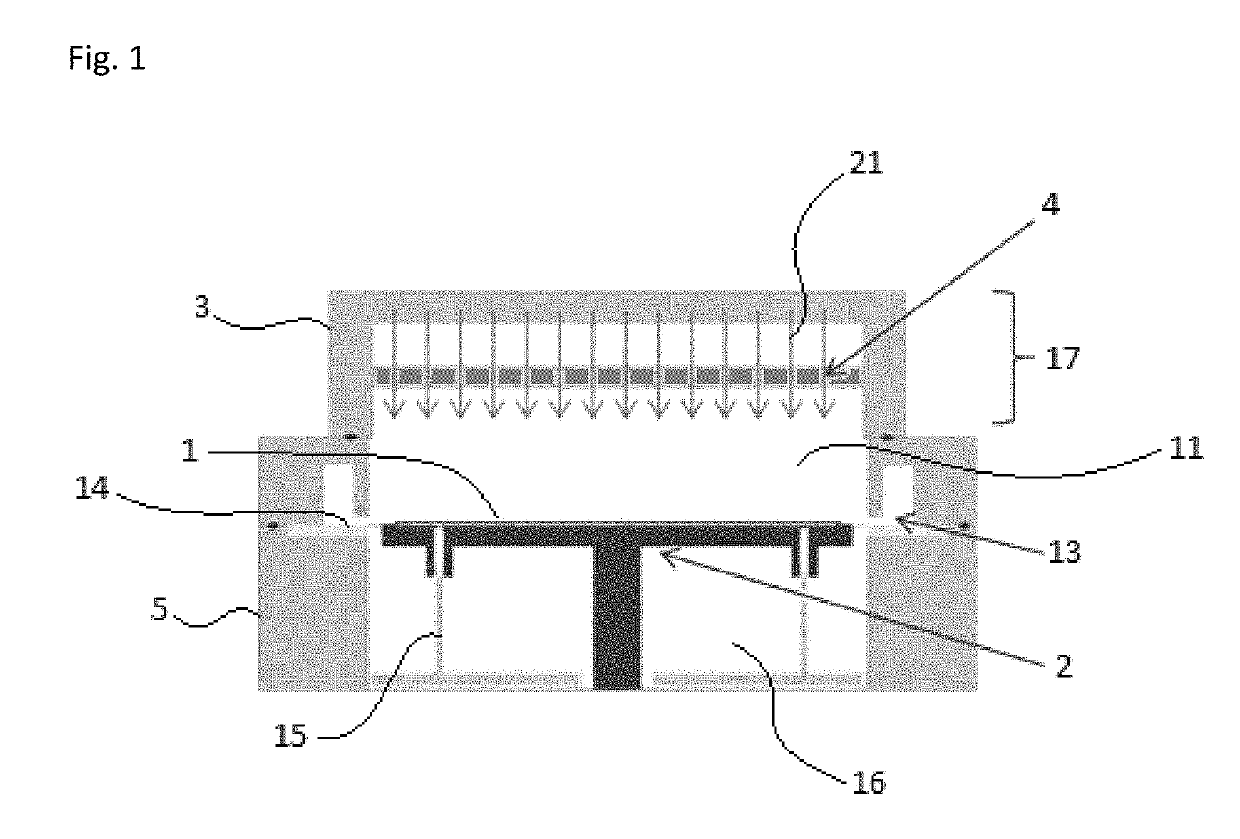
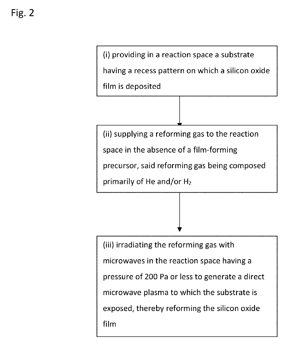
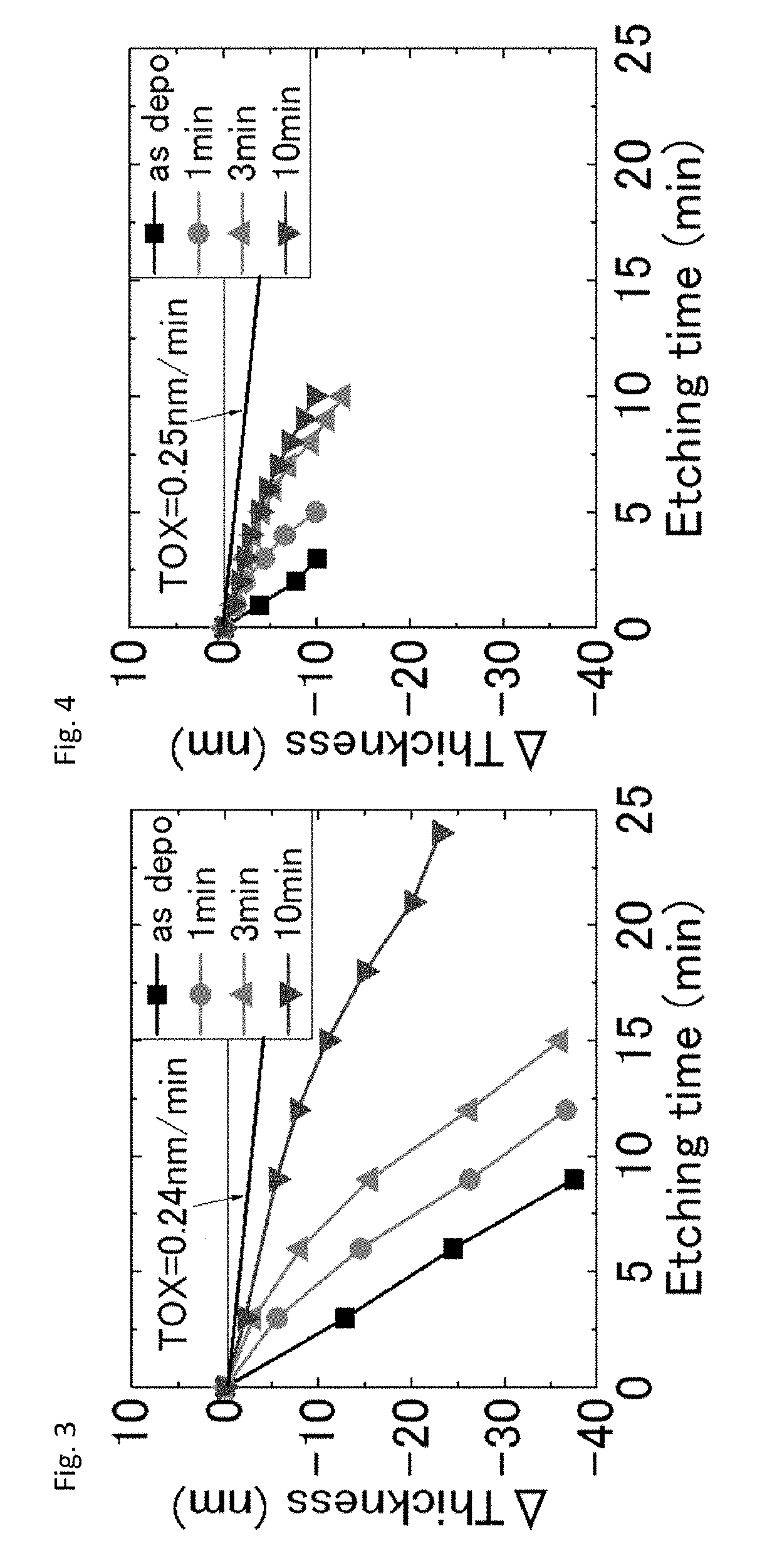
[0063]A substrate (having a diameter of 300 mm and a thickness of 0.7 mm) on which a silicon oxide film (a blanket film) having a thickness of 30 nm was deposited by PEALD was prepared. The substrate was loaded to the microwave apparatus illustrated in FIG. 1 and processed therein to reform the silicon oxide film using a sequence illustrated in FIG. 2 under conditions shown in Table 2 below. Helium gas was used as a reforming gas. Multiple films deposited on the substrates, respectively, were reformed for different reforming durations (1, 3, and 10 minutes) and then subjected to wet etching treatment under conditions shown in Table 3 below using an etching duration as a variable. Etched amounts of the silicon oxide films were measured to determine the film quality of each film.

TABLE 2(numbers are approximate)Conditions for Reforming StepPressure30 PaSubstrate temperatureRoom temperatureReforming gasHeFlow rate of reforming gas (continuous)100 sccmFrequency of microwaves2.45 GHzMicro...

example 2

[0066]Silicon oxide films deposited on substrates, respectively, were reformed and wet-etched in a manner substantially identical to that in Example 1, except that the film-reforming step was conducted at 200° C.

[0067]The results are shown in FIG. 4. FIG. 4 is a graph showing etched quantity (Δthickness) of silicon oxide film in relation to etching duration of the film before and after post-deposition reforming treatment using a He microwave plasma at 200° C. when varying the duration of reforming treatment. The graph of FIG. 4 also shows etched quantity (Δthickness =0.25 nm / min.) of thermal oxide film in relation to etching duration of the film as a reference etched quantity. As is shown in FIG. 4, as in FIG. 3, generally, the longer the reforming duration the less the etched quantity of the film per unit time became, i.e., the more the film reformation was manifested. Particularly, the etched quantity per unit time of the film reformed at 200° C. for 1 minute and that of the film ...

example 3

[0068]Silicon oxide films deposited on substrates, respectively, were reformed and wet-etched in a manner substantially identical to that in Example 2, except that film-reforming effect was determined as WERR (wet etch rate relative to that of thermal oxide film) when the etched quantity of each film was less than approximately 3 nm.

[0069]The results are shown in FIG. 6. FIG. 6 is a graph showing wet etch relative rate (WERR) of silicon oxide film in relation to etched depth of the film before and after post-deposition reforming treatment using a He microwave plasma when varying the duration of reforming treatment. As shown in FIG. 6, the film reforming was manifested from the surface to a depth of approximately 3 nm, and the WERR was as low as 2 to 4 when the reforming duration was 1 to 10 minutes, particularly as low as approximately 2 when the reforming duration was 3 to 10 minutes.


PUM

PropertyMeasurementUnit
Temperatureaaaaaaaaaa
Fractionaaaaaaaaaa

Abstract

A method of post-deposition treatment for silicon oxide film includes: providing in a reaction space a substrate having a recess pattern on which a silicon oxide film is deposited; supplying a reforming gas for reforming the silicon oxide film to the reaction space in the absence of a film-forming precursor, said reforming gas being composed primarily of He and / or H2; and irradiating the reforming gas with microwaves in the reaction space having a pressure of 200 Pa or less to generate a direct microwave plasma to which the substrate is exposed, thereby reforming the silicon oxide film.

Description

BACKGROUND OF THE INVENTIONField of the Invention[0001]The present invention is related generally to post-deposition treatment for silicon oxide film used in a semiconductor fabrication process.Description of the Related Art[0002]Recently, as miniaturization of Fin-FET structures and 3D technology of memory progress, a demand for high quality, high in-plane uniformity, and high conformality of silicon oxide film used in such processes becomes intense. Particularly, development of 3D V-NAND flash memories is remarkable, and demand for silicon oxide film which is applicable to a trench or hole having a high aspect ratio has increased every year.[0003]Conventionally, when an insulation film such as a gate oxide film, which is required to be high in insulating property and low in current leakage property, is deposited, a silicon oxide film is commonly deposited as such an insulation film by a thermal oxidation method (e.g., JP 2004-336019). However, since a high-temperature treatment pr...

Claims


Application Information

Patent Timeline
IPC IPC(8): H01L21/02H01L21/311
CPCH01L21/0234H01L21/02164C23C16/401H01L21/0228H01L21/31111H01L21/3105C23C16/402C23C16/56H01L21/28008H10B41/20H10B43/30H10B43/20H10B41/30H01L21/02274H01L21/02219H01J37/32192H01J37/3222H01J37/32623C23C16/50C23C16/45536H01L21/31105H10B69/00
Inventor SUZUKI, TOSHIYA
Owner ASM IP HLDG BV
Learn More