
Contact ring design for reducing bubble and electrolyte effects during electrochemical plating in manufacturing

a contact ring and electrolyte technology, applied in the field of electrochemical plating systems, can solve the problems of inability to meet the requirements of all applications, inhibit the plating reaction, and form no plating zones, etc., to improve drainage and fluid flow, improve the flow across the surface, and improve the effect of fluid flow

Active Publication Date: 2007-04-17
BELL SEMICON LLC
View PDF2 Cites 1 Cited by
  • Summary
  • Abstract
  • Description
  • Claims
  • Application Information

AI Technical Summary

Benefits of technology

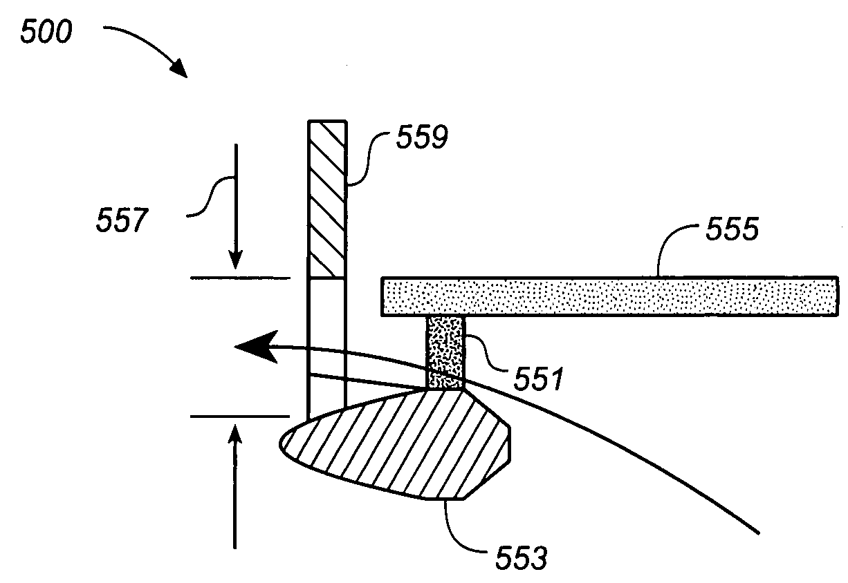
"The present invention provides contact ring designs and methods for reducing electroplating induced defects. The contact ring has openings that allow fluid to flow radially away from the ring, preventing the trapping of fluids between the substrate and the ring. The openings have aerodynamically streamlined flow surfaces to improve fluid flow. The invention also includes a toroidal contact ring with a support ring mounted on top of the ring base, which has sloped sides to aid in drainage of electrolyte. The support ring has a series of openings arranged along its circumference, enabling fluid flow from the inner edge of the ring to the outer edge of the ring. The cross-sectional shape of the openings is shaped like a wing. The technical effects of the invention are to reduce the incidence of electroplating induced defects and improve fluid flow during electroplating."

Problems solved by technology

However, current contact ring designs are not suitable for all applications.
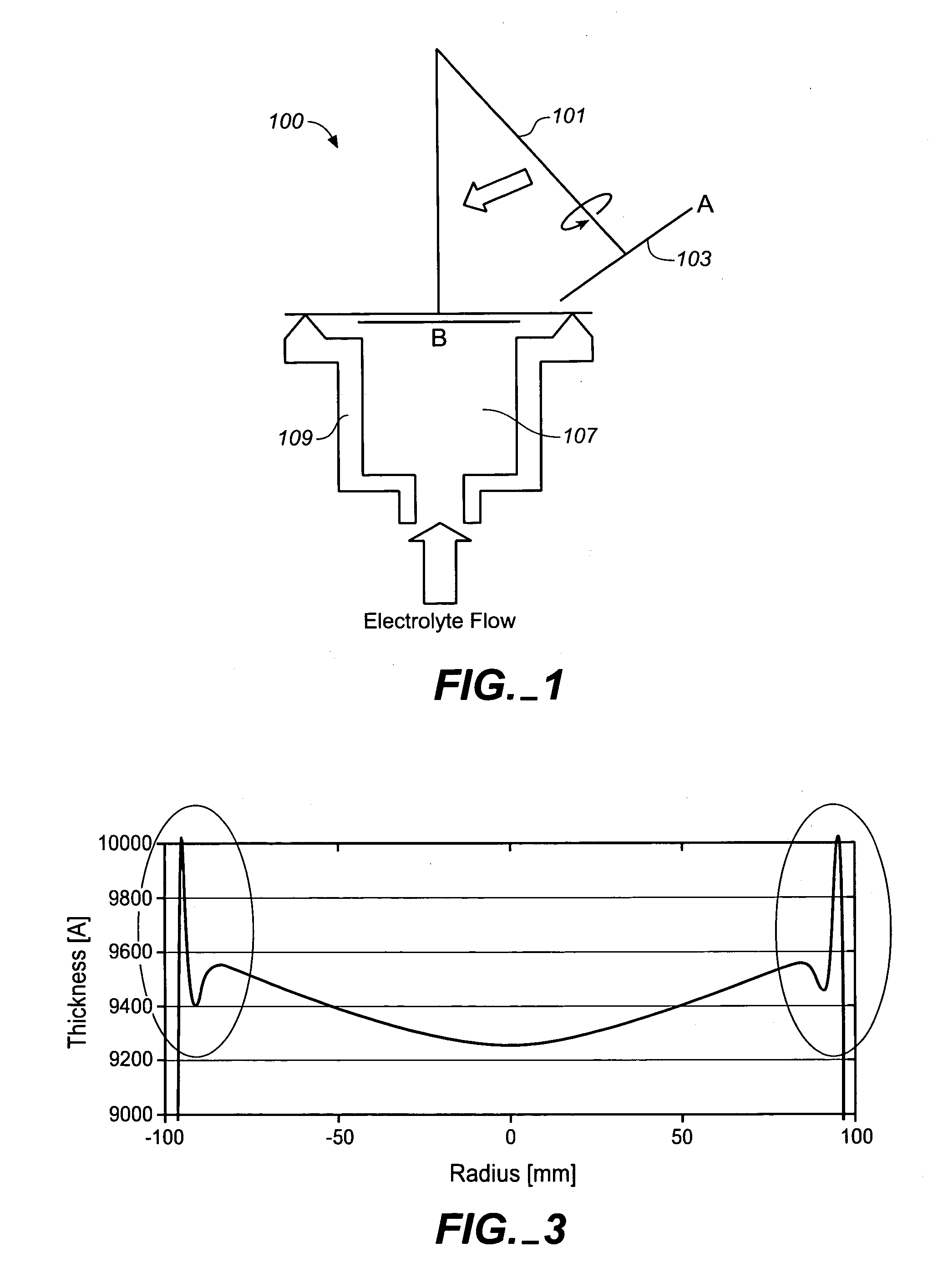
Bubble defects occur in areas where a large potential gap between the electrolyte and a wafer surface is created by bubbles in the electrolyte, inhibiting the plating reaction and leading to the formation of no plating zones.
Moreover, since the wafer is rotating, bubbles that form will often spiral out away from the point of formation, leaving swirl-shaped plating defects.
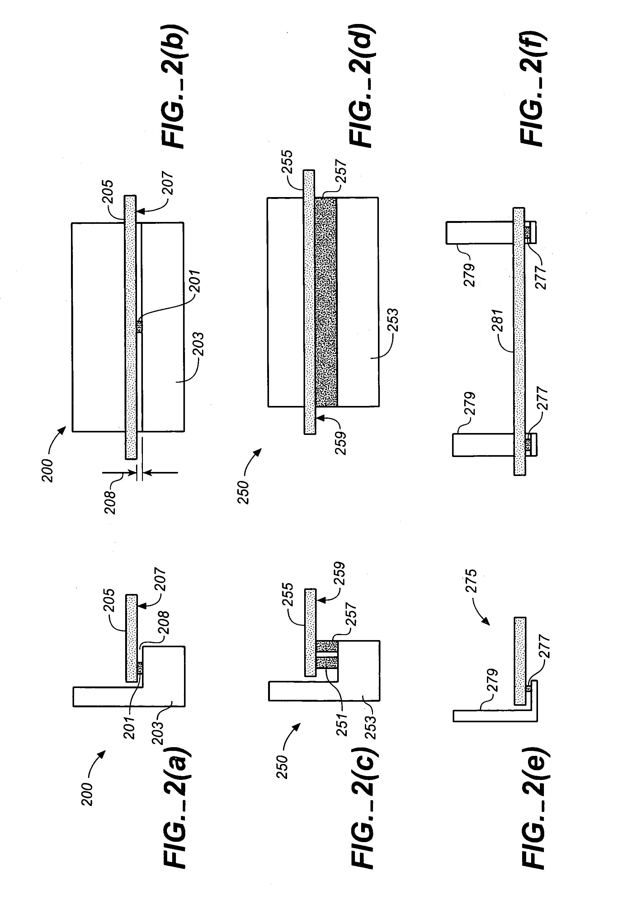
However, the dry contact ring design actually worsens the problem of bubble trapping when compared to the wet contact ring design because there is no place for trapped bubbles to escape once they have been formed.
One additional issue with using the dry contact ring design is that boundary conditions near the barrier 257 cause a localized increased thickness of electroplated material to be formed.
In order to remove the spikes at the edge of the electroplated material, the material must be over-polished, leading to increased erosion (sheet ρ variation) at the wafer center.
A first concern is that the robust electrical contact required for uniform distribution of current during electroplating may be hard to achieve due to the relatively weak support structure provided by individual support arms 279.
The additional stress and voltage tolerance requirements induce a need for more expensive materials.
However, implementing new methods results in additional hardware / control requirements as well as, potentially, a loss in throughput due to additional processing time.
On a side note, when using a dry contact ring, such as those discussed above in reference to FIGS. 2(c) and 2(d), a post-plating DI rinse is required before the wafer is removed from the wet section of the apparatus, because the electrolyte, if allowed to enter the dry portion of the plating chamber, will result in corrosion of components and create defects in the plated material due to corrosion particles and precipitation of inorganic salts from the electrolyte.
Another common problem that occurs with conventional contact ring designs is that of “trapped” residual electrolyte, which occurs when wafers are electroplated in succession.
Such electroplated defects can lead to topography differences, resulting in erosion and dishing defects after CMP has been completed. FIG. 4(a) is a photograph of a “scalloping” defect, while FIG. 4(b) shows an atomic force microscopy (AFM) scan across the defect, illustrating the ridge visible in the photograph.
A second, related problem occurs during the transfer stages after plating has been completed.
Electrolyte induced staining can result in erosion and dishing defects (similar to those caused by scalloping defects, discussed above) after CMP has been completed.
The foregoing discussion addresses some limitations of conventional contact ring designs, the use of which can result in potentially yield-impacting defects.

Method used


Image

  • Contact ring design for reducing bubble and electrolyte effects during electrochemical plating in manufacturing
  • Contact ring design for reducing bubble and electrolyte effects during electrochemical plating in manufacturing
  • Contact ring design for reducing bubble and electrolyte effects during electrochemical plating in manufacturing

Examples


Embodiment Construction

[0027]The invention pertains to an improved contact ring for use in electroplating a semiconductor substrate material (e.g., a semiconductor wafer). Specifically, the principles of the present invention are directed to improved contact ring designs and methods in order to minimize or eliminate common plating defects while maintaining the contact ring's structural strength and chemical resistance.

[0028]In the discussion above, several common problems with current contact rings were discussed. The solutions detailed in this various embodiments of the present invention generally address these problems. Some embodiments of the invention address improvements to fluid flow near the electrical contacts. One specific embodiment is shown in FIGS. 5(a)–5(d) and 6(a)–6(e).

[0029]In general, a contact ring according to various embodiments of the invention incorporates a number of changes from older designs. In one embodiment, openings are formed along the circumference of the contact ring. These...


PUM

PropertyMeasurementUnit
entry angleaaaaaaaaaa
entry anglesaaaaaaaaaa

Abstract

A contact ring for use in electroplating of a substrate material is constructed such that fluid (e.g., electrolyte) is allowed to flow radially away from the axis of a toroidal support ring, thus preventing the trapping of fluids between the substrate and the toroidal support ring. The contact ring is constructed with a series of openings arranged about the circumference of the ring and wherein an electrical contact is placed in the path of each opening so any fluid passing through the opening also passes around the associated electrical contact. Further, the electrical contacts are also placed such that a substrate (e.g., a semiconductor wafer) can be placed inside the support ring so as to electrically contact the electrical contacts. The toroidal support ring has an aerodynamically streamlined cross-section at the openings, such that fluid flows through the openings with reduced aerodynamic drag.

Description

BACKGROUND OF THE INVENTION[0001]1. Field of the Invention[0002]The present invention relates to electrochemical plating systems, and specifically addresses improvements over conventional “contact ring” designs.[0003]2. Description of the Related Art[0004]Copper has taken on a significant role in semiconductor integrated circuit (IC) manufacturing because of its low resistivity and the potential for improved electromigration (EM) performance as compared to aluminum. The current standard for copper metallization is electrochemical plating. One typical apparatus used in electroplating operations is a “contact ring”. However, current contact ring designs are not suitable for all applications.[0005]In conventional IC manufacturing processes, the apparatus used to electroplate material onto a substrate typically includes a plating cell 100 as shown in FIG. 1, which is a schematic diagram of a side view of a typical “fountain” type electroplating cell. FIG. 1 shows a support arm 101, whic...

Claims


Application Information

Patent Timeline
Patent Type & Authority Patents(United States)
IPC IPC(8): B23H3/04
CPCC25D5/04C25D17/06C25D21/04C25D7/123C25D17/001C25D5/003
Inventor KWAK, BYUNG-SUNG LEOPIATT, GREGORY FRANKMIZUNO, HIROSHI
Owner BELL SEMICON LLC
Learn More