Electrical scanning probe microscope apparatus

a microscope and scanning probe technology, applied in the direction of instruments, nuclear engineering, material analysis using wave/particle radiation, etc., can solve the problems of affecting the image distorted differential capacitance profiles, and perturbing the contrast of scm images, so as to improve the accuracy of junction images

Inactive Publication Date: 2007-03-20
NAT APPLIED RES LAB
View PDF9 Cites 9 Cited by
  • Summary
  • Abstract
  • Description
  • Claims
  • Application Information

AI Technical Summary

Benefits of technology

[0008]Accordingly, an object of the present invention is to provide an electrical scanning probe microscope apparatus comprising an atomic force microscope equipped with a long-wavelength laser to overcome the photoperturbation effects and improve the accuracy of junction images, in particular for ultra-shallow junctions in the narrower band-gap semiconductors.

Problems solved by technology

However, photoperturbations, such as the photovoltaic effect and the high-level carrier injection effect induced by stray light of the AFM red laser beam lead to distorted differential capacitance (dC / dV) profiles and hence perturb the contrast of SCM images.
The photoperturbations induced by the AFM laser beam not only affect the image contrast of SCM images, but also reduce the accuracy of the determination of the carrier concentration distribution.
Solutions to these problems have been long sought but thus far have eluded those skilled in the art.

Method used


Image

  • Electrical scanning probe microscope apparatus
  • Electrical scanning probe microscope apparatus
  • Electrical scanning probe microscope apparatus

Examples


Embodiment Construction

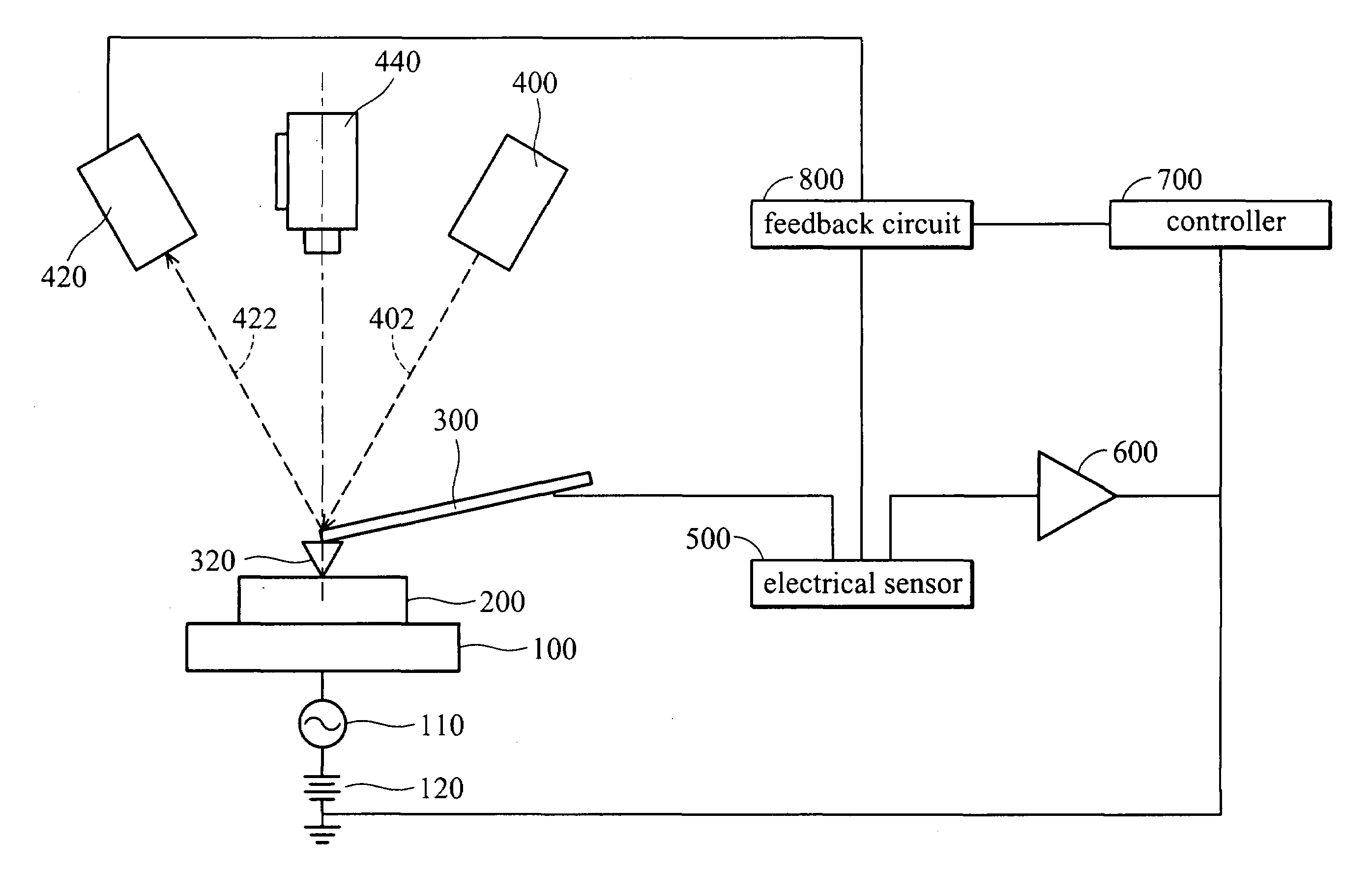
[0020]The present invention will be described with respect to preferred embodiments in a specific context, namely in a scanning capacitance microscope (SCM) apparatus. The invention may also be applied, however, to other applications, such as scanning spreading resistance microscopes (SSRM), Kelvin force microscopes (KFM) and conductive atomic force microscopes (C-AFM).

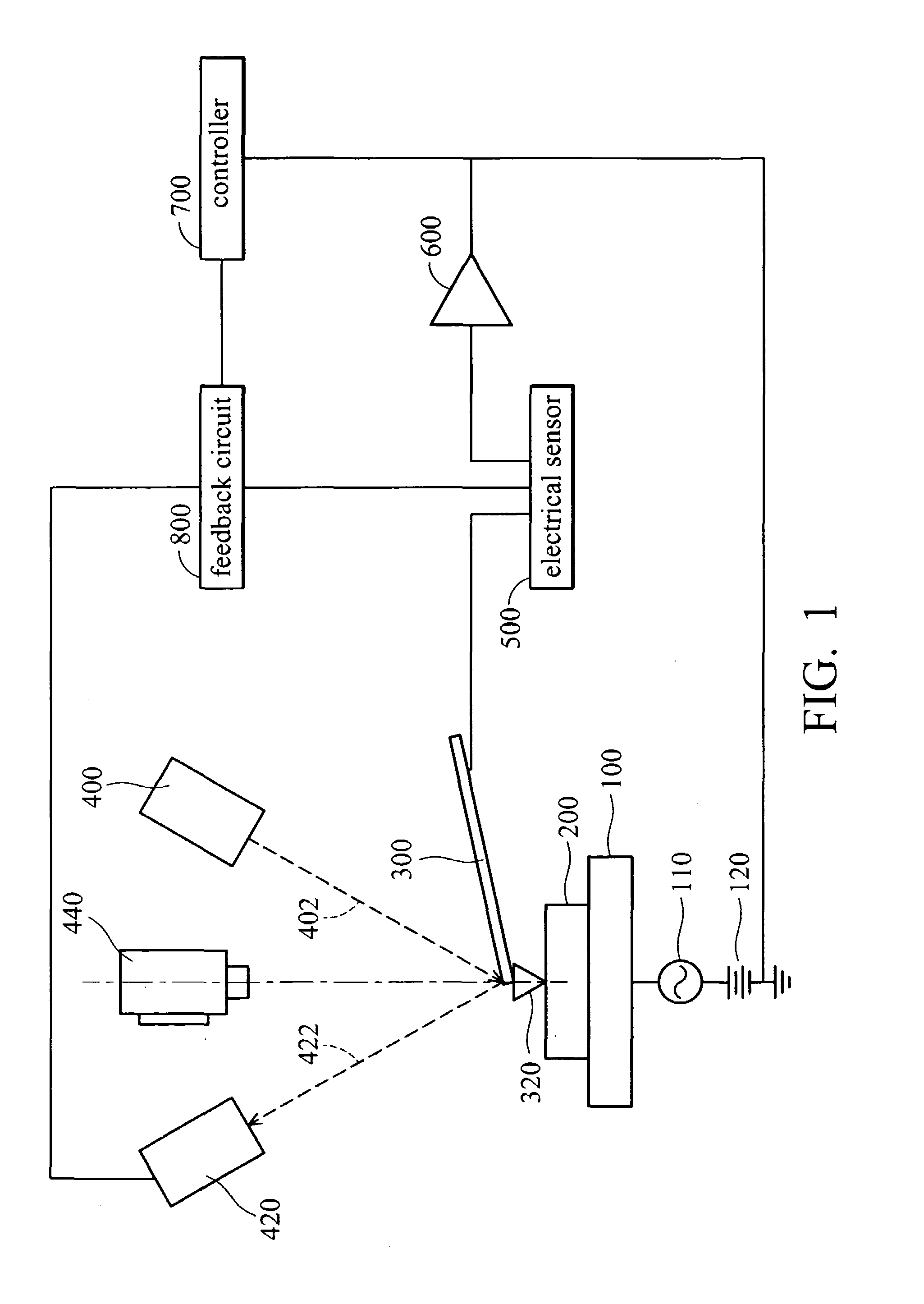
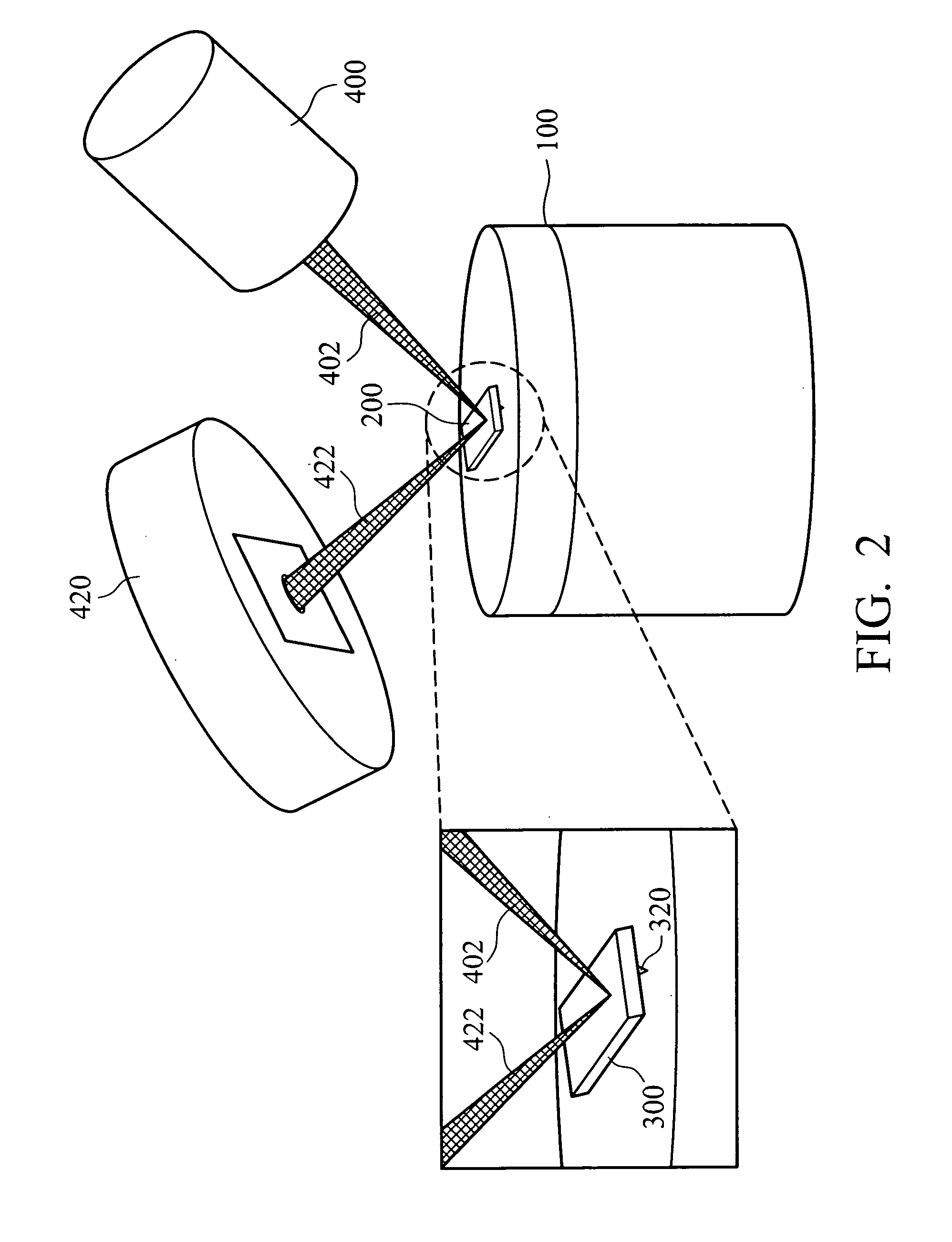
[0021]FIG. 1 is a functional block diagram of an electrical scanning probe microscope (SPM) apparatus according to an embodiment of the present invention. The (SPM) apparatus comprises an atomic force microscope with a long-wavelength laser as a surface image measuring setup to provide a topographic image and an electrical scanning sensor device to synchronously provide a two-dimensional electrical image. The electrical scanning sensor device comprises a capacitance sensor, a spreading resistance sensor, or a current sensor. The atomic force microscope is equipped with a long-wavelength laser source as a surface morph...


PUM


Abstract

An electrical scanning probe microscope (SPM) apparatus. The SPM apparatus is equipped with an atomic force microscope with an infrared laser source, a position-sensitive photo-detector (PSPD) to provide a topographic image, a charge-coupled device (CCD) monitor for optical alignment, and an electrical scanning sensor operatively coupled to the atomic force microscope to acquire synchronous two-dimensional electrical images. The photoperturbation effects induced by stray light and perturbation of the contrast of SCM images can thus be ameliorated.

Description

CROSS-REFERENCE TO RELATED APPLICATIONS[0001]This is a continuation-in-part of application Ser. No. 10 / 861,385, filed on Jun. 7, 2004 now U.S. Pat. No. 6,975,129, the teachings of which are incorporated herein by reference.BACKGROUND OF THE INVENTION[0002]1. Field of the Invention[0003]The invention relates to an electrical scanning probe microscope apparatus, and more particularly to an electrical scanning probe microscope apparatus comprising an atomic force microscope equipped with a long-wavelength laser source.[0004]2. Description of the Related Art[0005]Scanning probe microscopes (SPMs) providing very high resolution images of various surface properties are typically employed as a means of measuring surface topography and corresponding electrical property analysis. Different types of electrical properties can be measured such as, conductivity, voltage, capacitance, resistivity, current, and others. Accordingly, many different SPM techniques may be used when measuring electrica...

Claims


Application Information

Patent Timeline
Patent Type & Authority Patents(United States)
IPC IPC(8): G01R31/02G01Q10/00G01Q20/02G01Q60/02G01Q60/24G01Q60/40G21K7/00
CPCB82Y35/00G01Q20/02G01Q60/30G01Q60/40G01Q60/02
Inventor CHANG, MAO-NAN
Owner NAT APPLIED RES LAB
Why Eureka
Try Eureka