
High linearity and low noise CMOS mixer and signal mixing method

a mixer and signal technology, applied in the field of communication, can solve the problems of affecting the dynamic range of the communication system, affecting the system performance, and raising the noise floor component of the mixer output, so as to reduce third-order distortion, increase the gain of the rf signal, and increase the input intercept poin

Active Publication Date: 2007-02-13
APPLE INC
View PDF9 Cites 25 Cited by
  • Summary
  • Abstract
  • Description
  • Claims
  • Application Information

AI Technical Summary

Benefits of technology

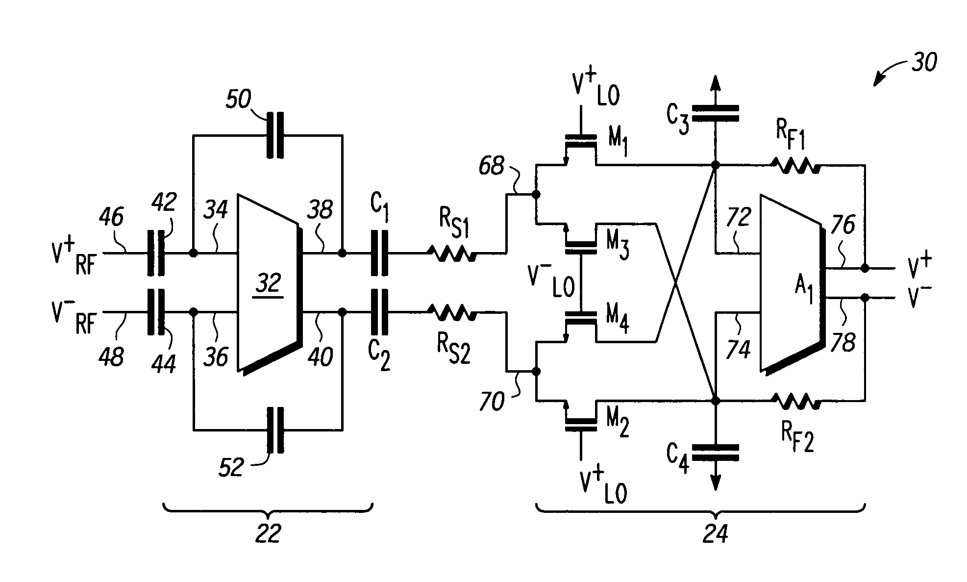
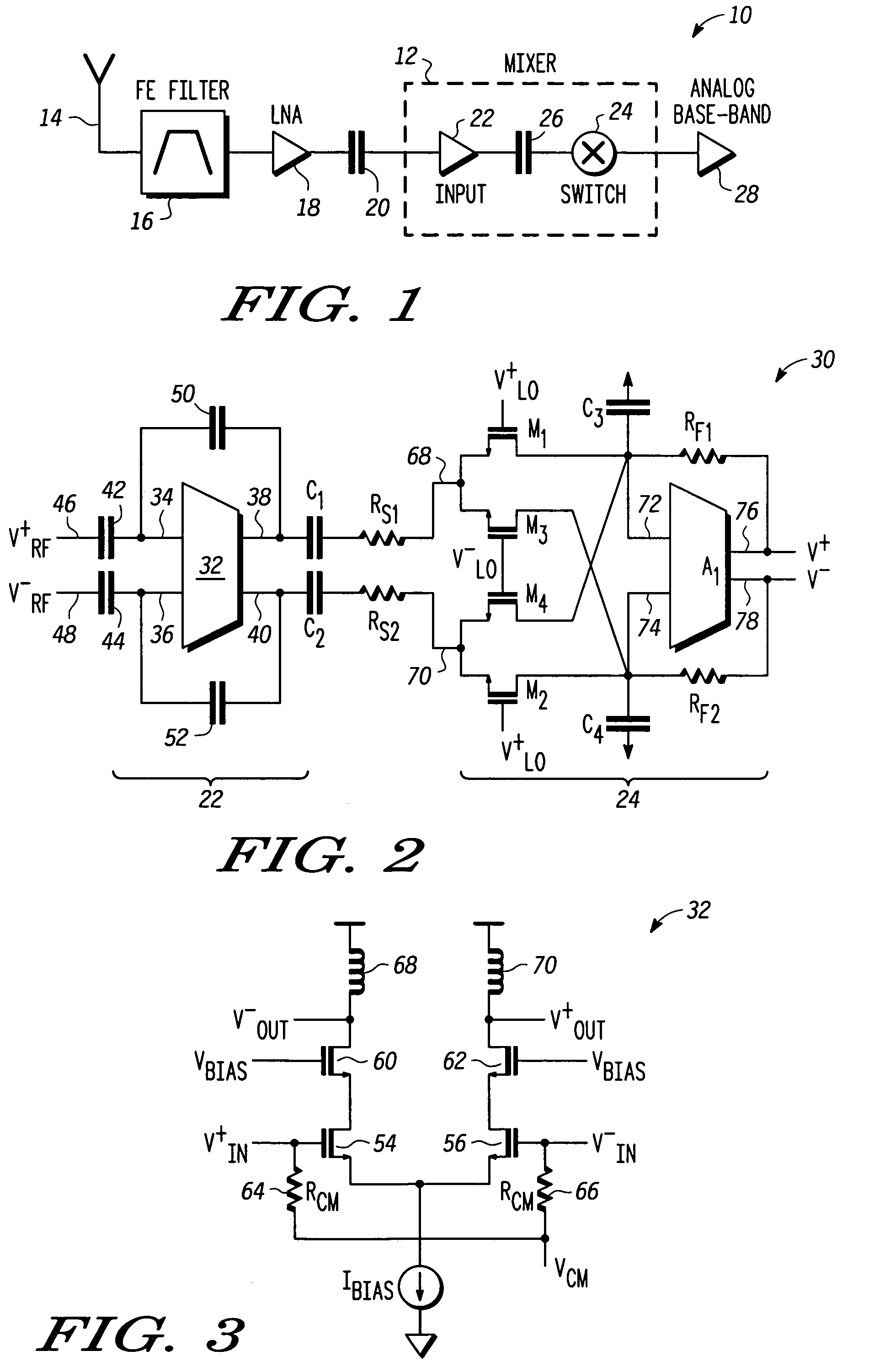
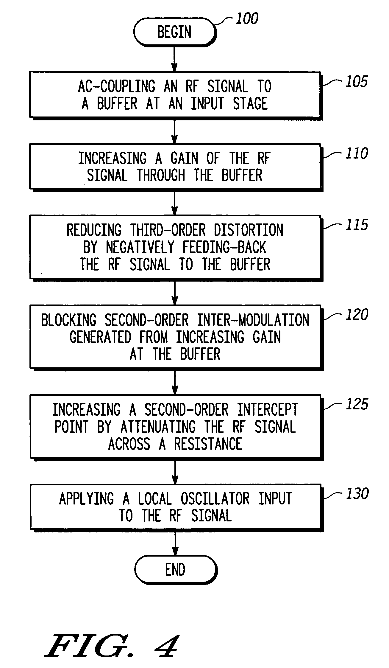
The patent describes an apparatus and method for reducing noise and distortion in a demodulated RF signal. The apparatus includes a mixer circuit with a coupling network, buffer, feedback network, blocking capacitor, input resistor, transistor based network switch, and operational amplifier. The method includes AC coupling, increasing gain, reducing distortion, blocking intermodulation, and applying a local oscillator input. The technical effects include improved linearity and reduced noise in RF signal processing.

Problems solved by technology

This distortion is usually caused by non-linear translations of the input signal and typically affects the dynamic range of the communication system.
The result of this may be a raised noise floor component of the mixer output.
The IM2 spurs are generally caused by mismatches of devices in the receiver architecture which may also occur in differential circuit topology.
For a direct-conversion receiver where a desired signal of interest is downconverted from RF to base-band through a single modulation process, interference from second-order nonlinearities, such as IM2, is usually detrimental to system performance.

Method used


Image

  • High linearity and low noise CMOS mixer and signal mixing method
  • High linearity and low noise CMOS mixer and signal mixing method
  • High linearity and low noise CMOS mixer and signal mixing method

Examples


Embodiment Construction

[0016]The following detailed description of the invention is merely exemplary in nature and is not intended to limit the invention or the application and uses of the invention. Furthermore, there is no intention to be bound by any theory presented in the preceding background of the invention or the following detailed description.

[0017]According to various embodiments, an apparatus is provided for a high linearity and low noise mixer. In one exemplary embodiment, the apparatus is a mixer circuit having a high linearity low noise mixer. Although the invention is described in the context of CMOS type transistors, a variety of transistors may be used including, by way of example and not of limitation, field effect transistors (FETs), bipolar transistors, and insulated gate bipolar transistors. The mixer circuit is ideally suited for low intermediate frequency (IF) or direct-conversion receiver architectures, such as used in fully integrated wireless receivers, and may be used in a wide ...


PUM


Abstract

Method and apparatus are provided for high linearity and low noise communication signal mixing. The apparatus includes a high linearity low noise mixer having an input stage coupled to a switch stage by a series-coupled blocking capacitance and input resistance. The input stage includes a buffer with negative feedback, and the switch stage includes a transistor based switch network connected to an amplifier that has feedback resistance and shunting capacitance. The method includes AC coupling an RF signal, increasing a gain of the RF signal, reducing third-order distortion by negatively feeding-back the RF signal, blocking IM2 generated from said gain increasing step, increasing a second-order input intercept point (IIP2) by attenuating the RF signal across a resistance, and applying a local oscillator input to the RF signal.

Description

FIELD OF THE INVENTION[0001]The present invention generally relates to communications, and more particularly relates to mixer circuits and related methods in communications.BACKGROUND OF THE INVENTION[0002]Mixer circuits, or mixers, are widely used in modern communication systems and have a number of uses. A typical application is for translating signals into desirable frequency bands through a technique called modulation. In a mixing or modulation process, an information signal is superimposed upon a carrier signal. In this way, the information signal may be processed or transmitted while minimizing, and at times without, information loss. Another principle application of mixer circuits is for demodulation. In demodulation, a modulated information signal is typically translated to an intermediate frequency.[0003]Mixers are generally designed to minimize inter-modulation (IM) distortion. This distortion is usually caused by non-linear translations of the input signal and typically a...

Claims


Application Information

Patent Timeline
Patent Type & Authority Patents(United States)
IPC IPC(8): G06F3/033H04B1/18
CPCH03D7/1441H04B1/30H03D7/1466H03D7/1458H03D2200/0088H03D2200/0025
Inventor CONNELL, LAWRENCE E.CUI, YANWAGH, POOJAN A.RAKERS, PATRICK L.
Owner APPLE INC
Learn More