Implantation process in semiconductor fabrication

a technology of semiconductor fabrication and implantation process, which is applied in the direction of semiconductor devices, electrical apparatus, transistors, etc., can solve the problems of increasing increasing junction leakage, and increasing performance and leakage. , to achieve the effect of reducing band-to-band tunneling and impact ionization, and reducing the number of transistors

Active Publication Date: 2007-02-06
INFINEON TECH AG
View PDF18 Cites 6 Cited by
  • Summary
  • Abstract
  • Description
  • Claims
  • Application Information

AI Technical Summary

Benefits of technology

[0005]In one aspect, the present invention provides an implant scheme that utilizes a main implant (pre-amorphization, species and co-implants) combined with a weak non-amorphizing “softening” implant (same or different species, with or without co-implant) placed slightly beyond the main implant. This softening implant moves, partly or fully, EoR defects within the junction, thereby removing them from the most critical location for leakage at the junction interface. Due to its non-amorphizing property, the softening implant will have slight diffusion (like a diffusion tail) that smoothens the junction and reduces band-to-band tunneling and impact ionization. Both effects reduce junction leakage. In optimized application, the overall increase in junction depth should be small.

Problems solved by technology

As the gate length is scaled down, it is becoming more and more difficult to adjust performance and leakage.
However, the drastically reduced thermal budget drives up junction leakage since it prevents the annealing of defects, mostly end-of-range (EoR) defects, and leads to extremely hard junctions, which increase band-to-band tunneling (BTBT) and impact ionization (II).

Method used


Image

  • Implantation process in semiconductor fabrication
  • Implantation process in semiconductor fabrication
  • Implantation process in semiconductor fabrication

Examples


Embodiment Construction

[0013]The making and using of the presently preferred embodiments are discussed in detail below. It should be appreciated, however, that the present invention provides many applicable inventive concepts that can be embodied in a wide variety of specific contexts. The specific embodiments discussed are merely illustrative of specific ways to make and use the invention, and do not limit the scope of the invention.

[0014]The present invention will be described with respect to preferred embodiments in a specific context, namely the formation of a field effect transistor. The invention may also be applied, however, to other processes that utilize ion implantation. For example, other semiconductor components such as bipolar transistors, capacitors, resistors and diodes can be formed using ion implantation processes.

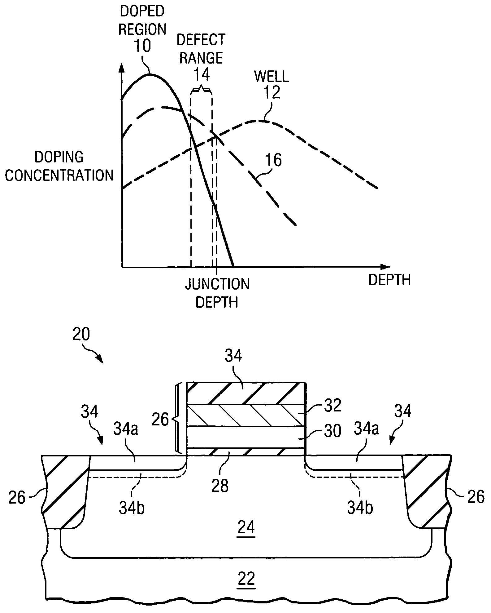
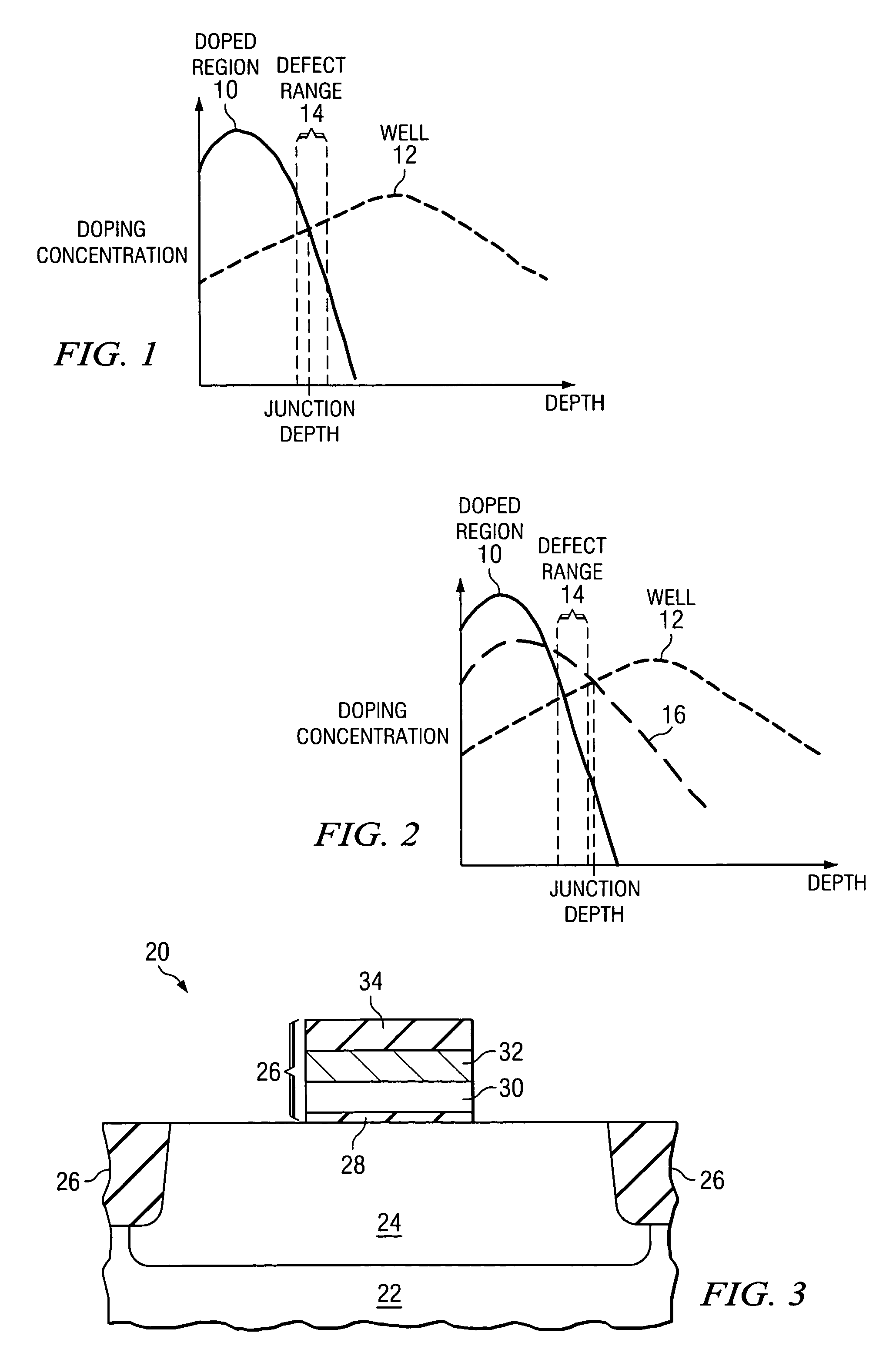
[0015]FIG. 1 illustrates a first graph that shows a single implant approach of forming a doped region in a semiconductor substrate. The x-axis provides the depth into the substr...


PUM


Abstract

A semiconductor device is formed by performing an amorphizing ion implantation to implant dopants of a first conductivity type into a semiconductor body. The first ion implantation causes a defect area (e.g., end-of-range defects) within the semiconductor body at a depth. A non-amorphizing implantation implants dopants of the same conductivity type into the semiconductor body. This ion implantation step implants dopants throughout the defect area. The dopants can then be activated by heating the semiconductor body for less than 10 ms, e.g., using a flash anneal or a laser anneal.

Description

TECHNICAL FIELD[0001]This invention relates generally to semiconductor processes, and more particularly to an implantation process in semiconductor fabrication.BACKGROUND[0002]Semiconductor devices are used in a large number of electronic devices such as computers, cell phones and others. One of the goals of the semiconductor industry is to continue shrinking the size of individual devices. Smaller devices can be fabricated more inexpensively (e.g., since more chips can be formed simultaneously on a single wafer) and can operate at higher speeds (e.g., since the physical distance between components is smaller). As a result, the continual shrinking of components, such as transistors, is desirable.[0003]One process that is commonly used to form semiconductor components is ion implantation. As an example, to form the source and drain of a transistor, dopant ions are typically implanted into a semiconductor body adjacent to a gate. These dopants must then be activated using a thermal pr...

Claims


Application Information

Patent Timeline
Patent Type & Authority Patents(United States)
IPC IPC(8): H01L21/425
CPCH01L21/26513H01L29/6659H01L21/26506H01L29/517H01L21/28052
Inventor HIERLEMANN, MATTHIAS
Owner INFINEON TECH AG
Why Eureka
Try Eureka