
One mask Pt/PCMO/Pt stack etching process for RRAM applications

a technology of etching process and mask, which is applied in the direction of basic electric elements, semiconductor/solid-state device manufacturing, electric apparatus, etc., can solve the problems of low etching rate, inability to etch portions of devices where etching is not desired, and little of the mask survives the etching process, etc., to achieve clean sidewalls and field, high selectivity

Inactive Publication Date: 2007-01-30
XENOGENIC DEV LLC
View PDF3 Cites 49 Cited by
  • Summary
  • Abstract
  • Description
  • Claims
  • Application Information

AI Technical Summary

Benefits of technology

"The patent describes a method for making a PCMO-containing RRAM device by using a single hard mask for etching. The method results in clean sidewalls and field, and has high selectivity between the hard mask and any underlying layer. The technical effects of this method include improved device performance and reliability."

Problems solved by technology

It has been reported that dry etching of PCMO using chemistries of chlorine and argon is somewhat workable, but the etch rate is very low and very little of the mask survives the etching process, leading to etching of portions of a device where etching is not desired.
It has also been reported that dry etching using pure argon to sputter etch the PCMO thin film has had some success, however, the same problem of poor selectivity of the PCMO thin film vs the mask material is present and unwanted etching of an underlying layer occurs.
A two-step, or multiple step, process has been used in the prior art, however, such techniques do not stop etching once the bottom electrode is reached, and results in residue being left on the stack sidewall, which residue is a direct result of etching the bottom electrode.

Method used


Image

  • One mask Pt/PCMO/Pt stack etching process for RRAM applications
  • One mask Pt/PCMO/Pt stack etching process for RRAM applications
  • One mask Pt/PCMO/Pt stack etching process for RRAM applications

Examples


Embodiment Construction

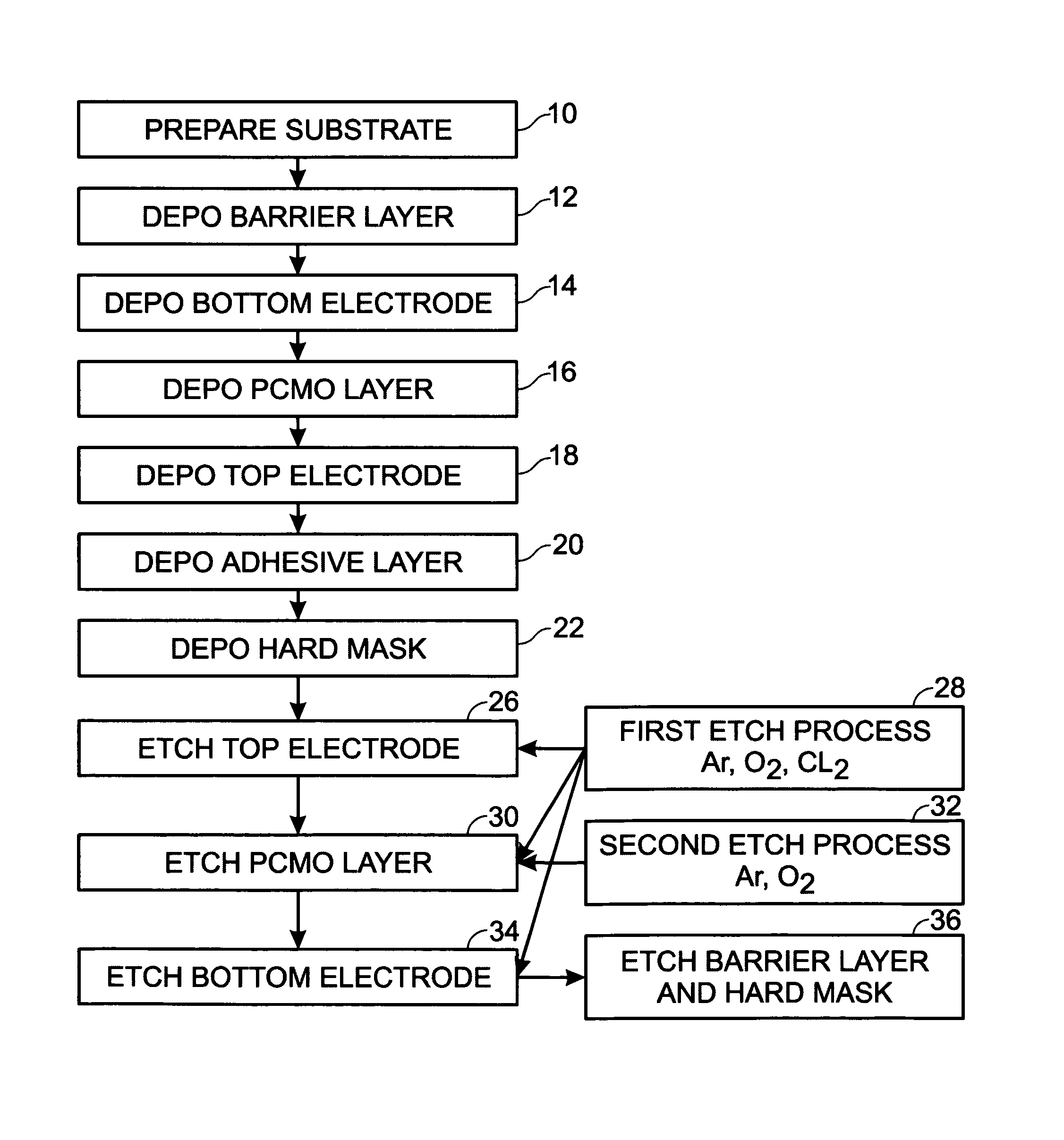
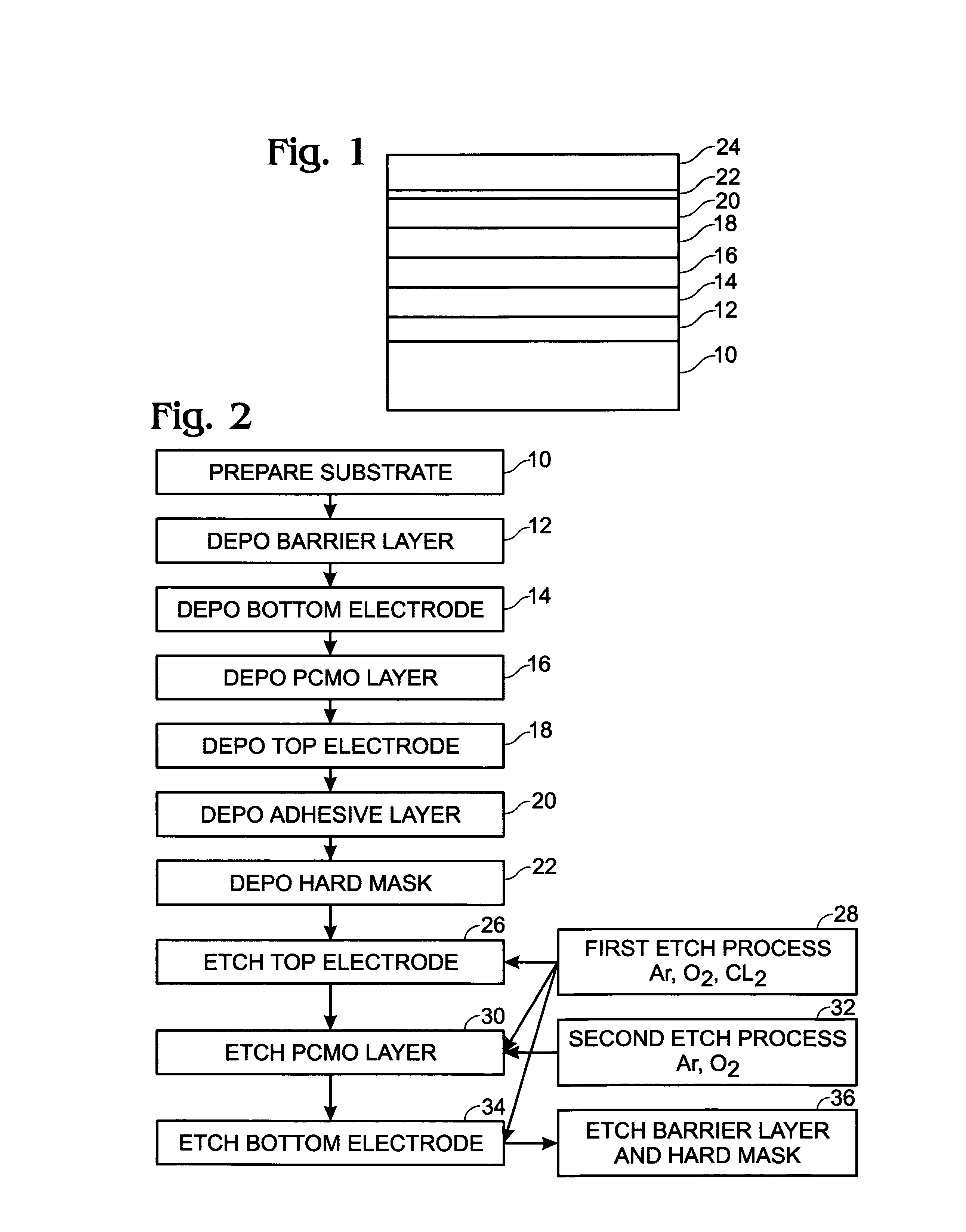
[0013]This invention resolves stack etching issues for electrode / perovskite / electrode stacks, such as Pt / PrxCa1-xMnO3 (PCMO) / Pt stacks, in that it minimizes the sidewall residue formed during an etching process. Two etching processes may be used in alternate steps during etching of a Pt / PCMO / Pt stack. The first etching process uses a gas mixture of Ar, O2, and Cl2, wherein Cl2 may be replaced by BCl3, CCl4, SiCl4, or combinations thereof. This process etches the platinum at a relatively high rate and results in less sidewall residue. In the case where platinum, or other noble metals, e.g., iridium or ruthenium, are used for both the top and bottom electrodes, this process is particularly suited for etching the top electrode and for etching the final portion of the PCMO, as the etching process approaches the bottom electrode. This process may also be used to etch a noble metal bottom electrode.

[0014]The second process uses a gas mixture of Ar and O2, and is essentially a sputtering p...


PUM

PropertyMeasurementUnit
RF bias poweraaaaaaaaaa
temperatureaaaaaaaaaa

Abstract

A one-mask etching method for use with a PCMO-containing RRAM to reduce stack side-wall residuals, includes preparing a substrate, taken from the group of substrates consisting of silicon, silicon dioxide and polysilicon; depositing a bottom electrode on the substrate; depositing a PCMO layer on the bottom electrode; depositing a top electrode on the PCMO layer; depositing a hard mask on the top electrode; depositing and patterning a photoresist layer on the hard mask; etching the hard mask; etching the top electrode using a first etching process having an etching atmosphere consisting of Ar, O2, and Cl2; etching the PCMO layer using an etching process taken from the group of etching processes consisting of the first etching process and a second etching process having an etching atmosphere consisting of Ar and O2. etching the bottom electrode using the first etching process; and completing the RRAM device.

Description

FIELD OF THE INVENTION[0001]This invention relates to etching processes, and specifically to a dry etching process for a Pt / PCMO / Pt stack for use in resistor random access memory (RRAM) applications. The method of the invention may also be applied to DRAMs, capacitors, sensors, optical displays, optical switches, transducers, imagers and other magnetic devices.BACKGROUND OF THE INVENTION[0002]PrxCa1-xMnO3 (PCMO) metal oxide is difficult to etch using a dry etching processes. It has been reported that dry etching of PCMO using chemistries of chlorine and argon is somewhat workable, but the etch rate is very low and very little of the mask survives the etching process, leading to etching of portions of a device where etching is not desired. It has also been reported that dry etching using pure argon to sputter etch the PCMO thin film has had some success, however, the same problem of poor selectivity of the PCMO thin film vs the mask material is present and unwanted etching of an unde...

Claims


Application Information

Patent Timeline
Patent Type & Authority Patents(United States)
IPC IPC(8): H01L21/06H01L21/461
CPCH01L45/1675H01L45/147H01L45/1233H01L45/04H10N70/20H10N70/826H10N70/8836H10N70/063
Inventor ZHANG, FENGYANSTECKER, LISA H.ULRICH, BRUCE D.HSU, SHENG TENG
Owner XENOGENIC DEV LLC
Learn More