Light emitting device
a technology of light-emitting devices and substrates, which is applied in the direction of discharge tubes luminescnet screens, organic semiconductor devices, nanoinformatics, etc., can solve the problems of difficult cracking of films on plastic substrates, and achieve the effect of preventing deterioration of substrates and flexible substrate structures
- Summary
- Abstract
- Description
- Claims
- Application Information
AI Technical Summary
Benefits of technology
Problems solved by technology
Method used
Image
Examples
embodiment 1
[Embodiment 1]
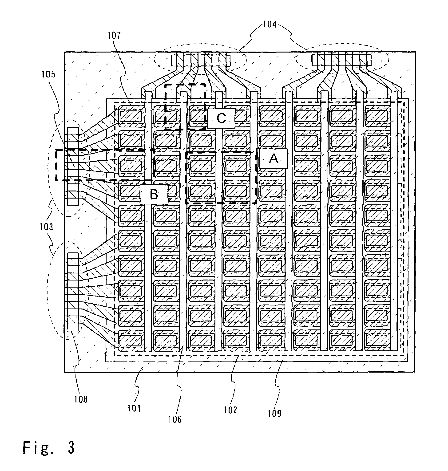
[0051]In this embodiment, a light emitting device is of a simple matrix type, in which light emitting elements are arranged in a matrix form to constitute a display screen. In this embodiment, we will describe an embodiment of sealing structure for protecting the light emitting elements from external contaminations such as oxygen and water vapor.
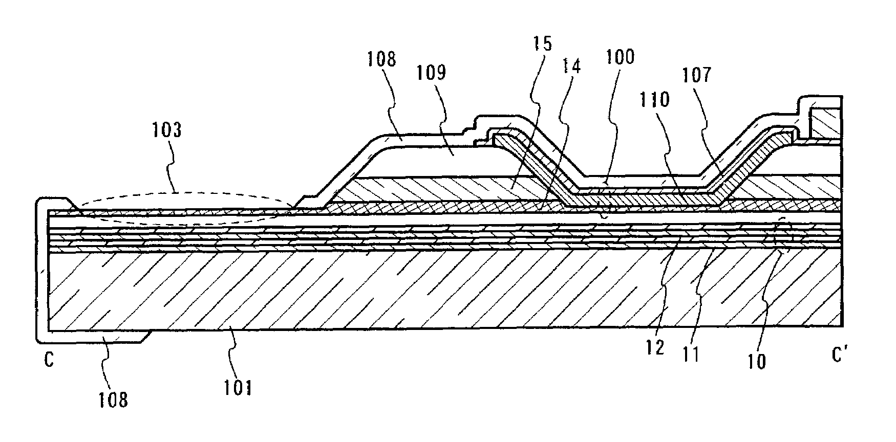
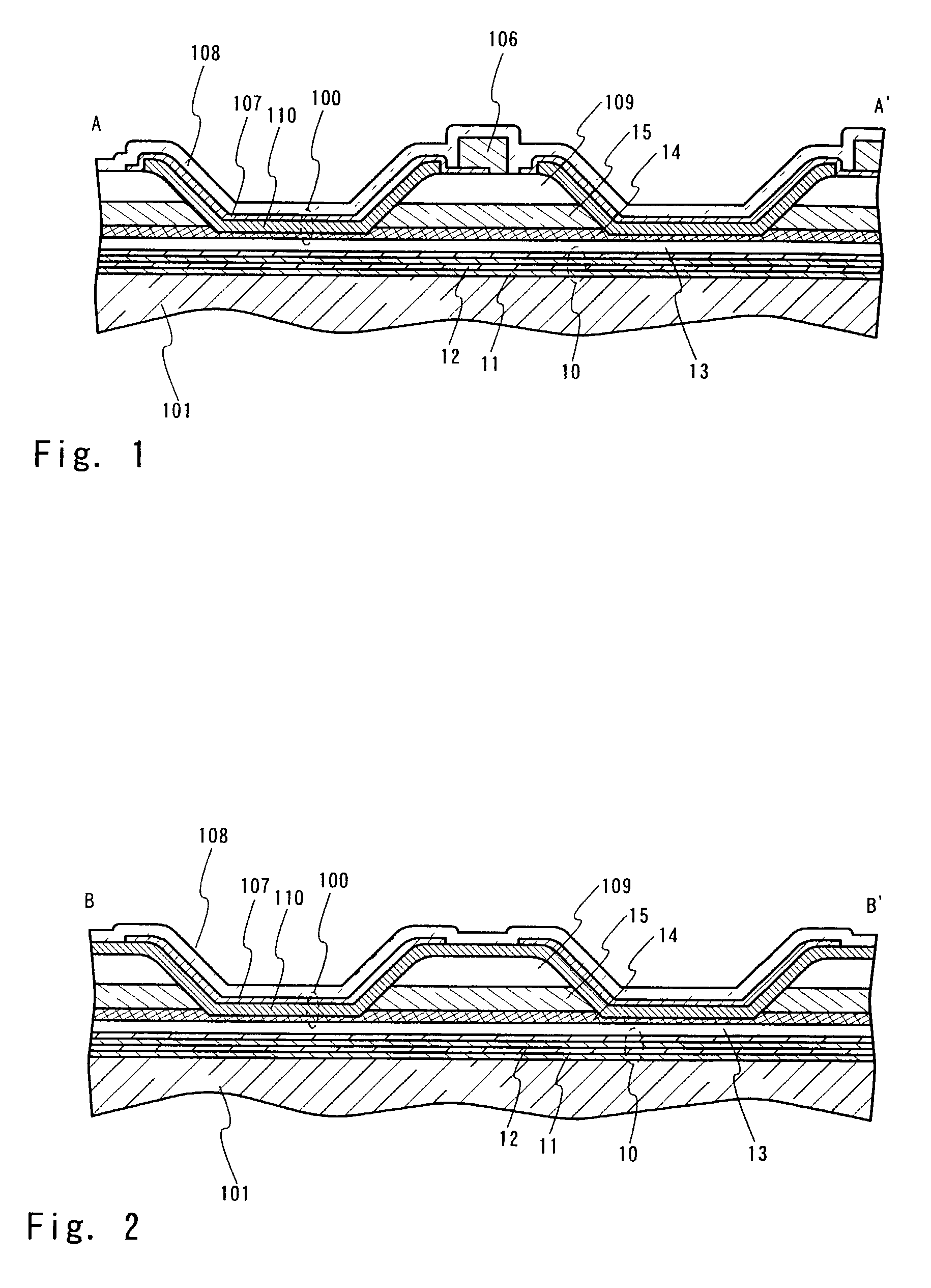
[0052]FIG. 3 is a top view for illustrating the configuration of the sealing structure. As shown in the figure, a pixel portion 102 is formed, where light emitting elements are arranged in a matrix form on a substrate 101. The pixel portion 102 includes a first wiring 105 in a stripe form extending in the X direction and a second wiring 106 in a stripe form extending in the Y direction. A first electrode 107 of the light emitting element is electrically connected to the second wiring 106. The stripe-formed first wiring 105 in the X direction and the stripe-formed second wiring 106 in the Y direction form their respective signal...
embodiment 2
[Embodiment 2]
[0080]In this embodiment, a light-emitting device is in the type of an active matrix in which a light emitting element and a TFT for controlling the light emitting element are arranged on each pixel to drive. In this embodiment, we will describe an embodiment of sealing structure for preventing the light emitting elements and TFTs from external contaminations such as oxygen and water vapor.
[0081]FIG. 13 is a top view for illustrating a pixel structure of the light emitting device, showing an exemplified configuration thereof in which a TFT and a light emitting element are mounted. FIG. 14 is a vertical cross sectional view along the line E–E′ in FIG. 13. Therefore, the present embodiment will be described with reference to these figures. Furthermore, in FIG. 13, the upper layers on a second electrode (i.e., a partition wall layer, an EL layer, a first electrode, and an inorganic compound layer) are omitted for a simplification of the drawing.
[0082]As shown in the figur...
embodiment 3
[Embodiment 3]
[0095]Various kinds of electronic apparatus can be implemented with the light emitting device of the present invention described above. Typical electronic apparatus includes personal digital assistants (i.e., electronic notes, mobile computers, cellular phones, and electronic books and magazines), video cameras, digital cameras, cellular phones, and so on. Some of these examples are shown in FIG. 20.
[0096]In FIG. 20A, there is shown an example of a video camera implemented by the application of the present invention. The video camera comprises a main body 3011, a display part 3012, a voice input part 3013, an operation switch 3014, a battery unit 3015, and a viewing part 3016. Accordingly, the present invention allows the implementation of such a light-weighted video camera.
[0097]In FIG. 20B, there is shown an example of a personal digital assistant (PDA) implemented by the application of the present invention. The PDA comprises a main body 3031, a stylus pen 3032, a d...
PUM
 Abstract
Description
Claims
Application Information
 - R&D
- Intellectual Property
- Life Sciences
- Materials
- Tech Scout
- Unparalleled Data Quality
- Higher Quality Content
- 60% Fewer Hallucinations
Browse by: Latest US Patents, China's latest patents, Technical Efficacy Thesaurus, Application Domain, Technology Topic, Popular Technical Reports.
© 2025 PatSnap. All rights reserved.Legal|Privacy policy|Modern Slavery Act Transparency Statement|Sitemap|About US| Contact US: help@patsnap.com


