
10 Gbit/sec transmit structure with programmable clock delays

a transmission structure and clock delay technology, applied in the field of repeaters in high-speed data transmission, can solve the problems of limiting the large-scale use of optical networks to increase data bandwidth, affecting the growth of transmission bandwidth, etc., and achieve the effect of suppressing power/ground noise generation and low inductan

Active Publication Date: 2007-01-02
TEXAS INSTR INC
View PDF8 Cites 19 Cited by
  • Summary
  • Abstract
  • Description
  • Claims
  • Application Information

AI Technical Summary

Benefits of technology

[0014]The present invention provides a robust solution to the task of re-aligning data in the transmit portion of an optical-electrical-optical repeater system and offers flexibility in the circuit board design approach. A single high performance analog phase locked-loop circuit is used to simultaneously provide clock / data recovery for multiple bit streams. The power dissipation required to perform clock recovery is thereby reduced to a fraction of that required in conventional transmit systems.
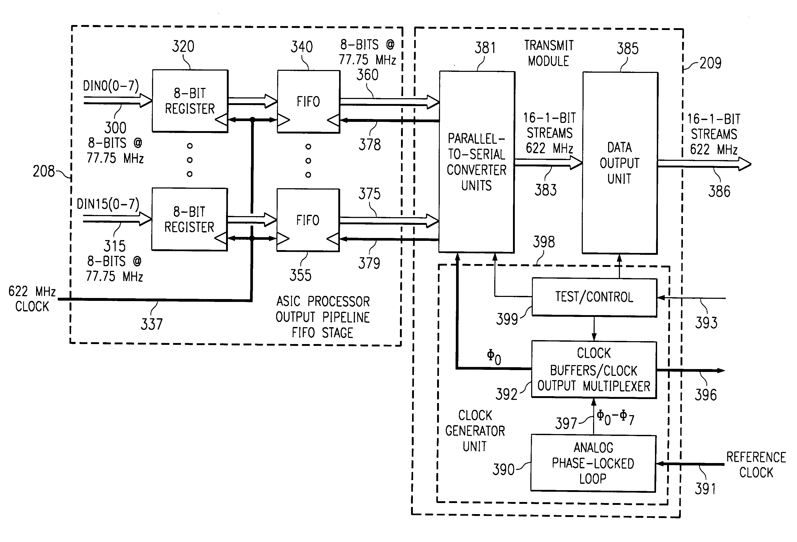
[0015]This invention relates specifically to the transmit module which includes: a clock recovery circuit having an analog phase-locked loop (APLL) with multiple phase outputs; parallel-to-serial conversion blocks; output buffers with programmable output voltage swings; control logic for selecting frequency multiplication ratio and output phases; and liberal distribution of power and ground pads to assure low inductance, high conductance power feed to the high frequency circuits and to suppress power / ground noise generation in high speed switching elements.

Problems solved by technology

The required use of bipolar Gallium-Arsenide technology with ASIC technology in the same repeater represents a technology mismatch and has hindered the growth of transmission bandwidth in optical networks.
Thus the power dissipation of such a conventional multi-technology electrical-optical repeater system as well as the technology mismatch limits their large-scale use to increase data bandwidth.

Method used


Image

  • 10 Gbit/sec transmit structure with programmable clock delays
  • 10 Gbit/sec transmit structure with programmable clock delays
  • 10 Gbit/sec transmit structure with programmable clock delays

Examples


Embodiment Construction

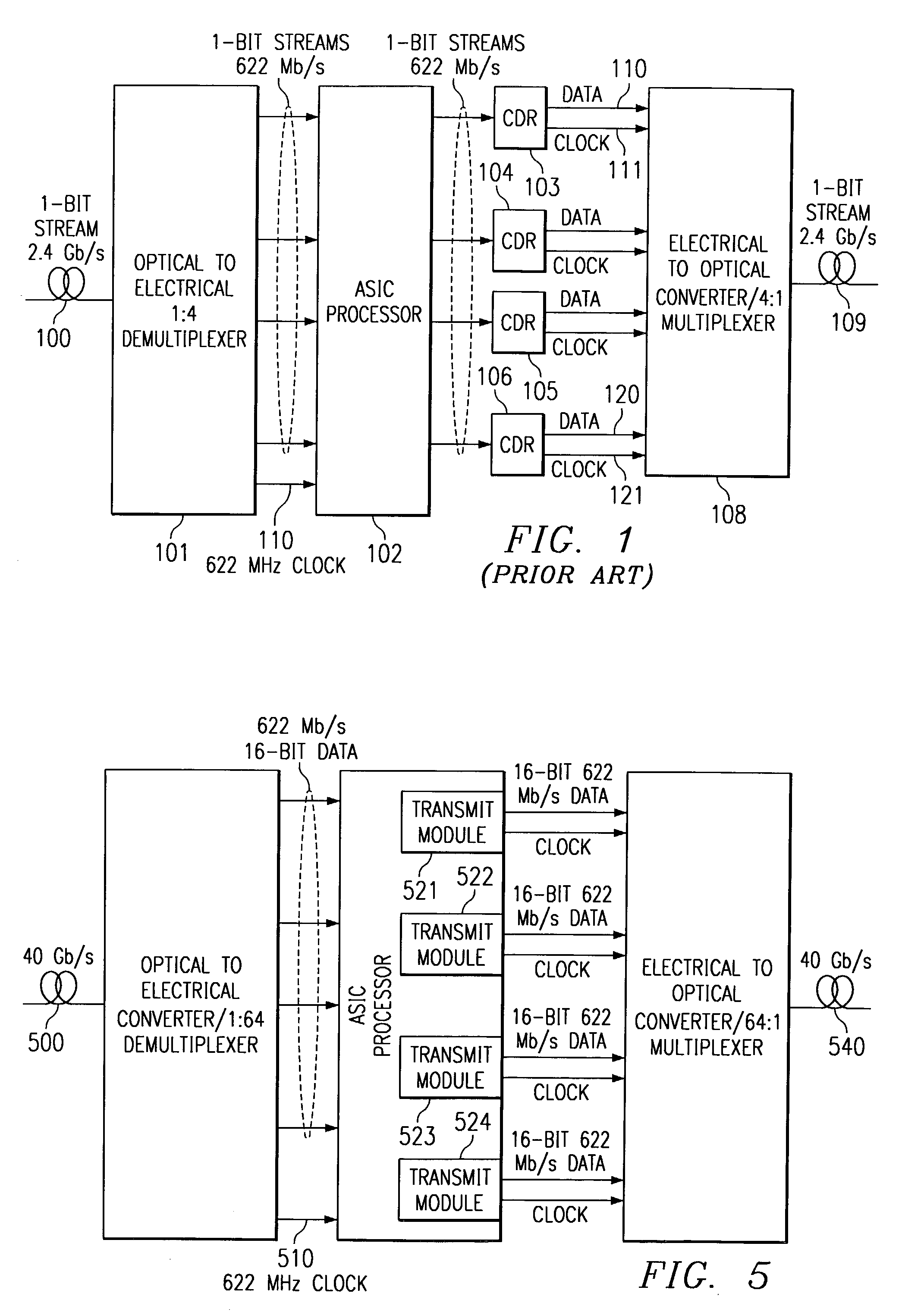
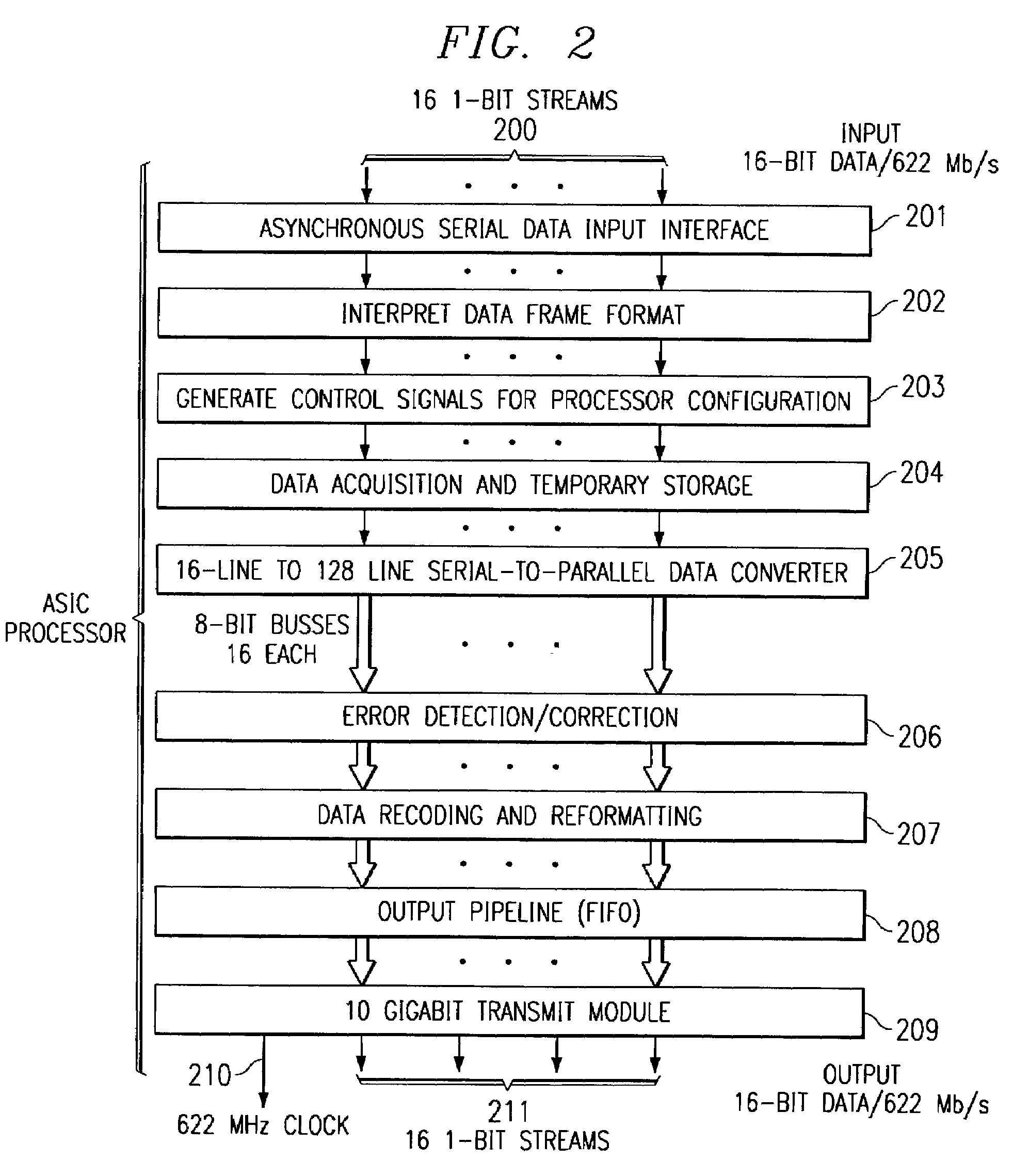
[0022]FIG. 2 illustrates the block diagram of an ASIC processor flow which incorporates the preferred embodiment of the invention, an OC-192 performance level 10 Gb / sec transmit module. At a 10 Gb / sec data stream rate, the optical-to-electrical converter is required to demultiplex by a factor of 16, resulting in 16 1-Bit data streams each at 622 MHz arriving at the input to the ASIC processor. The conventional ASIC processor functions listed earlier are illustrated in FIG. 2 along with the transmit module 209 of this invention. The width of the processor pipeline for the 10 Gb / sec repeater system is four-times larger than that of the conventional 2.4 Gb / s system. The 4-bit wide data stream input of the 2.4 Gb / sec system increases to 16-bits in width. Corresponding to the 32-bit parallel width of the 2.4 Gb / sec system, the parallel width at 10 Gb / sec is 128 bits.

[0023]The system uses an all complementary metal oxide semiconductor (CMOS) application specific integrated circuit (ASIC) ...


PUM


Abstract

The present invention provides a robust solution to the task of re-aligning data at the transmit end of a fiber optic or other high performance serial link, and also offers flexibility in the circuit board design approach. A high performance analog phase locked-loop circuit is used to simultaneously provide clock recovery for multiple bit streams. The power dissipation required to perform clock recovery is thereby reduced to a fraction of that required in conventional transmit systems. This analog phase locked loop produces plural phase output signals. An output multiplexer selects one phase for use in electrical to optical conversion.

Description

[0001]This application claims priority under 35 USC §119(e)(1) of Provisional Application No. 60 / 340,207, filed Dec. 12, 2001.TECHNICAL FIELD OF THE INVENTION[0002]The technical field of this invention is repeaters in high speed data transmission.BACKGROUND OF THE INVENTION[0003]Data transmission at extremely high rates is conventionally carried out by means of serial data streams arranged into packets or frames. Fiber Optic line transmission is becoming increasingly popular at rates of 10 G bits / sec and above.[0004]Conversion and realignment of Sonet OC-192 based standard data streams at 10 Gbit / sec from optical to electrical and then back to optical is an essential part of the process of realizing any high-speed switch fabric in the optical networking discipline. This is because the optical data signals passed from one location to another suffer attenuation in the transmission lines and must be refreshed at intervals in the transmission. This is done by means of receive-transmit m...

Claims


Application Information

Patent Timeline
IPC IPC(8): H04B10/00H03L7/18H04B10/17H04B10/29H04J3/06H04Q11/04
CPCH03L7/18H04J3/0685H04B10/29H04J2203/0089
Inventor PATHAK, VIJAY KUMARPARTHASARATHY, BHARADWAJDEVALAPALLI, SRINATH
Owner TEXAS INSTR INC
Learn More